Progettazione e produzione di stackup di PCB a 16 strati
I circuiti stampati (PCB) a 16 strati sono diventati un vettore tecnologico fondamentale per l'integrazione di sistemi complessi. La loro progettazione e produzione comporta un controllo preciso degli intercalari e la gestione dell'integrità del segnale. Queste schede multistrato bilanciano perfettamente i requisiti di cablaggio ad alta densità e di integrità del segnale attraverso una precisa struttura laminata.
Indice per materie
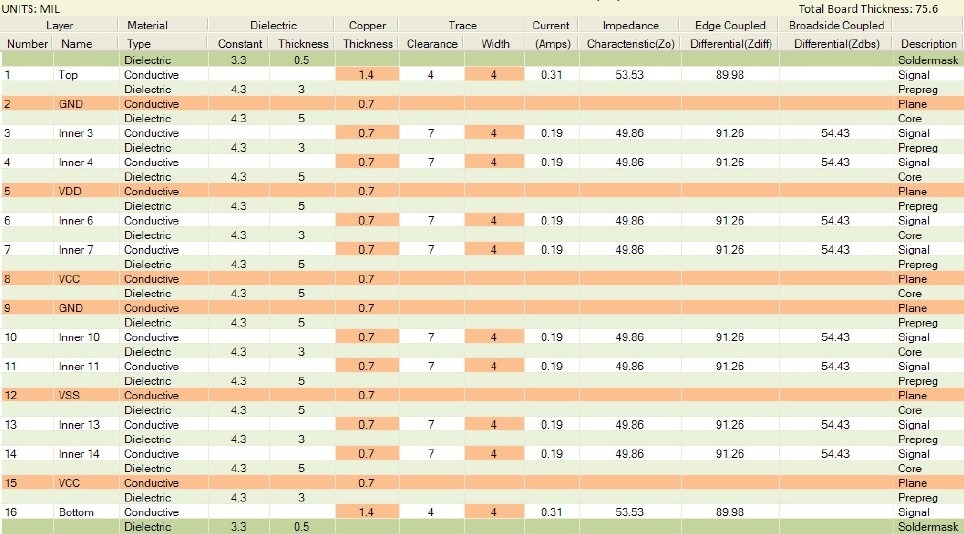
Struttura tipica del laminato di una scheda PCB a 16 strati
Configurazione 1: Segnale ad alta velocità ottimizzato (8S4P4G)
L1: Segnale (TOP) L2: GND L3: Segnale L4: Segnale
L5: PWR1 L6: GND L7: Segnale L8: Segnale
L9: PWR2 L10:GND L11:Segnale L12:Segnale
L13:PWR3 L14:GND L15:Segnale L16:GND(BOT)vantaggi:
- Ogni strato di segnale ha un piano di riferimento adiacente
- I piani di alimentazione divisi consentono di ottenere domini di tensione multipli
- Adatto per collegamenti seriali ad alta velocità da 56Gbps+
Configurazione 2: Tipo di elaborazione a segnale misto
L1: Segnale RF L2: GND L3: Analogico L4: PWR
L5: Digitale L6: GND L7: Digitale L8: PWR
L9: Digitale L10:GND L11:Digitale L12:PWR
L13:Analogico L14:GND L15:RF L16:GNDcaratteristiche:
- Circuiti RF e analogici con schermatura perimetrale
- Instradamento del segnale digitale su strati interni
- Ideale per le apparecchiature di imaging medicale
Configurazione 3: Tipo di applicazione ad alta potenza
(Include strati di alimentazione in rame da 2 oz di spessore e strati termici dedicati)Punti chiave:
- Strati di potenza in rame spessi 3OZ
- Strati termici con nucleo metallico incorporato
- Progettato per gli inverter EV
Raccomandazione dell'esperto: Eseguire simulazioni di campo elettromagnetico 3D quando si selezionano le configurazioni di stackup. Per la convalida del progetto si consiglia Ansys HFSS o CST Studio Suite.
Tecnologia dei materiali critici e controllo dello spessore
1. Selezione di materiali di alta gamma
| Tipo di materiale | Modello tipico | Dk@10GHz | Df@10GHz | domande |
|---|---|---|---|---|
| FR4 ad alta velocità | Megtron6 | 3.7 | 0.002 | 112G SerDes |
| Materiale a bassa perdita | RO4835 | 3.5 | 0.003 | Radar a onde millimetriche |
| Materiale altamente tg | IT-180A | 4.3 | 0.012 | Elettronica automobilistica |
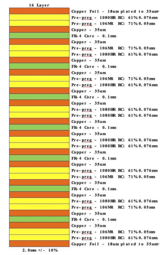
2.Sistema di controllo dello spessore
Esempio di spessore del pannello di 1,6 mm:
- Rivestimento in ramedello stratodi segnale: 1OZ (35μm)
- Rivestimento in rame: 2OZ (70 μm)
- Spessore dielettrico: 0,1 mm (4mil)
- Preimpregnato: tipo 1080
- Strato di controllo dell'impedenza: 0,2 mm (8mil)
Formula di calcolo:
Spessore totale = Σ(spessore del rame)+ Σ(spessore del dielettrico) + spessore della maschera di saldatura
Flusso del processo di produzione avanzata
- Tecnologia di foratura laser:
- Laser CO2: fori >100μm
- Laser UV: microfori inferiori a 100 μm
- Cieco tramite rapporto d'aspetto: 1:0.8
- Processo di placcatura a impulsi:
- Spessore del rame del foro: ≥25μm
- Uniformità superficialedel rame:±3μm
- Precisione di foratura posteriore: ±50μm
- Parametri critici di laminazione:
- Temperatura: 180 ± 5°C
- Pressione: 350 PSI
- Durata: 90 minuti
- Livellodi vuoto: <50 mbar
Standard di ispezione della qualità:
- IPC-6012B Classe 3
- IPC-A-600G
- 100% test della sonda volante
- Ispezione a raggi X 3D
Progettazione dell'integrità del segnale
- Tre elementi del controllo dell'impedenza:
- Tolleranza larghezzalinea ±10%
- Tolleranza dello spessore dielettrico ±7%
- Tolleranza dello spessore del rame ±1μm
- Progettazione dell'integrità di potenza:
- Capacità del piano >500 pF/pollice quadrato
- Posizionamento del condensatore di disaccoppiamento:
- 0,1 μF@0402 per BGA
- 10μF@0603 per dominio di tensione
- Strategie di ottimizzazione EMC:
- Vie di schermatura dei bordi: distanza<λ/20
- Slot diisolamento: larghezza >50mil
- Struttura a terra a sandwich
Studio di caso: Una AAU per stazione base 5G che utilizza PCB a 16 strati ha ottenuto una perdita di inserzione inferiore del 32%, prestazioni termiche migliori del 28% e un'affidabilità MTBF di 100.000 ore.
Servizi di produzione professionali raccomandati
Topfast offerte soluzioni chiavi in mano per PCB a 16 strati:
✅ Impilaggio personalizzato fino a 32 strati
✅ Controllo dell'impedenza ±5%
✅ Vie cieche laser da 100 μm
✅ Prototipi rapidi stampati in3D
✅ Servizi completi di simulazioneSI/PI
Ottenere un preventivo personalizzato immediato: Invia i requisiti tecnici
Punti salienti di FQA
D: Come bilanciare costi e prestazioni nei progetti a 16 strati?
A: Raccomandata “4+8+4” laminazione ibrida: 4 strati di materiale ad alta velocità + 8 strati di FR4 riducono il costo del 15% mantenendo le prestazioni critiche dello strato di segnale.
D: Come affrontare le sfide termiche nei pannelli a 16 strati?
R: Tre soluzioni efficaci:
- Blocchi di rame integrati per il raffreddamento locale
- Array termici di vie
- Materiali compositi ad anima metallica
D: Difetti comuni nella produzione di massa di schede a 16 strati?
R: Aree di intervento principali:
- Disallineamento da strato a strato
- Crepe di rame nei vial
- Vuoti negli strati dielettrici
- Finitura superficiale non uniforme
Applicazioni dei PCB a 16 strati
I circuiti stampati a 16 strati bilanciano perfettamente le esigenze di instradamento ad alta densità con i requisiti di integrità del segnale grazie a precise strutture di impilamento, trovando applicazioni diffuse nei settori della tecnologia:
- Infrastruttura di comunicazione 5G: Apparecchiature per stazioni base che supportano la trasmissione a onde millimetriche e la tecnologia MIMO massiva
- Calcolo ad alte prestazioniInterconnessioni tra processori per server e supercomputer AI
- Apparecchiature di imaging medicale: Sistemi di controllo per TAC, risonanza magnetica e altri dispositivi medici avanzati
- Elettronica aerospaziale: Soluzioni affidabili per le comunicazioni satellitari e i sistemi di controllo di volo
- Elettronica automobilisticaControllori di dominio per la guida autonoma e i sistemi smart cockpit
Parametri tecnici tipici:
- Spessore del pannello: 1,6-2,4 mm (personalizzabile)
- Larghezza/spazio minimo delle linee: 3/3mil (0,075/0,075mm)
- Apertura minima:0,15 mm (foratura laser)
- Tolleranza di allineamento trastrati:±25 μm
- Precisione del controllo dell'impedenza: ±7%
Approfondimento sul settore: Con l'adozione delle tecnologie PCIe 5.0 e DDR5, il mercato dei PCB a 16 strati sta crescendo del 12% all'anno e si prevede che supererà i 5,8 miliardi di dollari a livello globale entro il 2025.
Consultate ora i nostri esperti: Scarica il libro bianco sui PCB a 16 strati


Messaggi correlati