Guida completa ai PCB flessibili: tipi, progettazione e applicazioni
Indice per materie
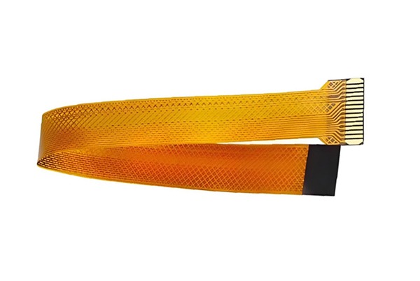
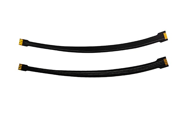
Che cosa PCB flessibili?
I circuiti stampati flessibili (FPC) utilizzano substrati flessibili come il poliimmide per resistere a piegature, flessioni o torsioni, rendendoli ampiamente applicabili per scenari di integrazione ad alta densità e flessione dinamica. Le caratteristiche principali includono:
- Leggero e sottile: Riduzione del 60% in termini di peso e spazio rispetto ai PCB rigidi.
- Capacità di flessione dinamica: Resiste fino a 500milioni di piegature ripetute (angolo completo di 360°).
- Adattabilità ambientale: Resistente alle alte temperature (fino a 400 °C), alle vibrazioni e alla corrosione chimica.
Confronto tra i tipi di PCB flessibili
| tipo | Caratteristiche strutturali | domande | Complessità produttiva |
|---|---|---|---|
| PCB flessibile su un solo lato | Poliimmide monostrato + foglio di rame + rivestimento protettivo | Connettori semplici, sensori | ★☆☆☆☆ |
| PCB flessibile a doppia faccia | Strati di rame su entrambi i lati + interconnessioni placcate con fori passanti | Cruscotti automobilistici, comandi industriali | ★★★☆☆ |
| PCB flessibile multistrato | ≥3 strati di rame + interconnessioni complesse | Dispositivi medici, strumenti aerospaziali | ★★★★★ |
Parametri tecnici chiave
1. Calcolo del raggio di curvatura
Formula: Raggio minimo di curvatura =(spessore della tavola× coefficiente di flessibilità) / 2
- Valore tipico: una scheda dello spessore di0,4mm può raggiungere una curvatura di 90°.
- Linee guida di sicurezza: raggio di curvatura consigliato ≤1 mm; le curve a 180° richiedono una progettazione speciale.
2. Composizione dei materiali
- Substrato: Principalmente poliimmide (PI), eccellente resistenza alle alte temperature.
- direttore: Rame laminato ricotto (flessione dinamica) vs. Rame elettrodepositato (applicazioni statiche).
- Materiali adesivi: Laminati in resina acrilica/epossidica.
Linee guida per la progettazione dei rinforzi
Posizionamento funzionale:
┌──────────────────────────────┐
│Supporto meccanico │ Previene la deformazione dell'area del connettore │
├──────────────────────────────┤
│ Dispersione delle sollecitazioni │ Riduce le sollecitazioni meccaniche sui giunti saldati │
├──────────────────────────────┤
│ Posizionamento di montaggio │ Fornisce un'interfaccia di montaggio rigida │
└──────────────────────────────┘
Materiali comuni: FR4 (0,2-0,5 mm), acciaio inossidabile (applicazioni ad alta frequenza).
Linee guida di progettazione (lista di controllo strutturata)
Layout traccia
- Evitare tracce ad angolo retto (utilizzare transizioni curve).
- Scaglionare le posizioni delle tracce sugli strati superiore e inferiore per le schede a doppia faccia.
- Aggiungere cuscinetti a goccia alle aree critiche per rinforzarle.
Manipolazione dell'area di curvatura
- Utilizzare riempimenti tratteggiati invece di riempimenti in rame solido.
- Vietare vie/pad nelle aree di curvatura.
- L'apertura della copertura dovrebbe essere più grande del 10% rispetto allo strato conduttore.
Considerazioni relative alla produzione
- Durante il montaggio dei pannelli è necessario lasciare un margine di 5 mm per il bordo.
- Specificare la tolleranza di spessore di ±0,1 mm per i connettori ZIF.
- Aggiungere segni di allineamento ottico.
Analisi dei vantaggi e dei limiti
Aree di vantaggio:
- ✅ Capacità di instradamento tridimensionale(risparmio di spazio del 40%).
- ✅ Resistenza alla fatica meccanica (durata 3 volte superiore in condizioni di vibrazione).
- ✅ Stabilità alle alte temperature(valore Tg >200 °C).
Limiti dell'applicazione:
- ⚠️ Il costo è superioredel 30-50% rispettoai PCB rigidi.
- ⚠️ Difficile da riparare (richiede attrezzaturespecializzate).
- ⚠️ Sensibile ai graffi (richiede un imballaggioprivodi zolfo).
Distribuzione delle applicazioni industriali
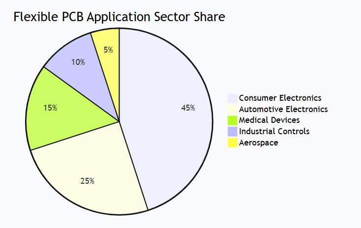
Scenari tipici:
- Smartwatch: connessionidisplay pieghevoli a 360°.
- Sistemi ADAS: circuiti sensori resistenti alle vibrazioni.
- Endoscopi: trasmissione di segnali biologici ad alta densità.
Note speciali sul processo di produzione
- Selezione di fogli di rame:
- Applicazioni dinamiche: rame laminato ricotto (RA) per una migliore duttilità.
- Applicazioni statiche: rame elettrodepositato (ED) per un costo inferiore.
- Finitura superficiale:
- ENIG: Massima affidabilità dei giunti saldati.
- OSP: Adatto per cicli di stoccaggio brevi.
- Placcatura in oro duro: dedicata ai connettori ZIF.
- Controllo qualità:
- Prova di flessione: verificata secondo lo standard IPC-6013.
- Prova di stress termico: resistenza della saldatura a288 °C.
- Controllo dell'impedenza: tolleranza richiesta ±10%.
Perché non sono adatti a tutte le situazioni?
Nonostante i notevoli vantaggi, le soluzioni rigide sono consigliate per:
Consiglio professionale: discutere con i produttori in merito alla DFM (Design for Manufacturability, progettazione per la producibilità) durante la fase di progettazione concettuale può ridurre i rischi di sviluppo di oltre il 30% e ottimizzare i costi di produzione. Il successo dell'applicazione dei PCB flessibili dipende dal coordinamento preciso tra la scelta dei materiali, la progettazione meccanica e i processi di produzione.


Messaggi correlati