PCB üretimi bir çok aşamalı, sıkı kontrol edilen süreç Küçük sapmaların güvenilirlik sorunlarına, verim kaybına veya maliyet artışına yol açabileceği yerlerde.
Birçok kaynak PCB üretimini yüksek düzeyde açıklasa da, PCB üretimini anlamak her üretim adımının bir sonraki adımla nasıl etkileşime girdiği için kritiktir:
- Üretilebilir panoların tasarlanması
- Maliyet kontrolü
- Uzun vadeli güvenilirliğin sağlanması
Bu makale bir PCB üretim sürecine adım adım genel bakışHer bir kritik aşamanın derinlemesine açıklamalarına bağlantılar içerir.
Perspektif, aşağıdaki gibi profesyonel PCB üreticileri tarafından kullanılan gerçek üretim uygulamalarını yansıtmaktadır TOPFASTProses istikrarı ve verim kontrolünün temel öncelikler olduğu yerlerde.
İçindekiler
Genel Bakış PCB Üretim Süreci
Tipik bir PCB üretim iş akışı şunları içerir:
- İç katman imalatı
- Delme (mekanik veya lazer)
- Bakır kaplama
- Desen aşındırma
- Muayene ve verim kontrolü
Her adım bir öncekinin üzerine inşa edilir. Sürecin başlarında yapılan hatalar genellikle daha sonra düzeltilemez.
İç Katman İmalatı
İç katman imalatı çok katmanlı PCB üretiminin temeli.
Bu aşamada:
- Bakır folyo iç devreler oluşturmak için desenlenmiştir
- Boyutsal doğruluk kritik öneme sahiptir
- Hatalar laminasyondan sonra kalıcı olarak yığına kilitlenir
İç katmanlar lamine edildikten sonra tamir edilemediğinden, üreticiler sıkı süreç kontrolleri ve denetim standartları uygulamaktadır.
İç katman hazırlama, görüntüleme ve aşındırma işlemlerinin ayrıntılı bir açıklaması için bkz:
İç Katman İmalatı Açıklandı
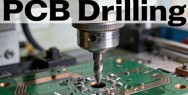
PCB Delme: Ara Katman Bağlantıları Oluşturma
Delme işlemi, daha sonra vialara ve delik bağlantılarına dönüşecek olan delikleri oluşturur.
İki temel sondaj yöntemi kullanılmaktadır:
- Mekanik delme
- Lazer delme
Her yöntemde ödünleşimler vardır:
- Delik boyutu
- En boy oranı
- Maliyet
- Güvenilirlik
Yanlış delme, kaplama kalitesini ve güvenilirliği doğrudan etkiler.
Mekanik delme veya lazerli delmenin ne zaman uygun olduğunu anlamak için okuyun:
PCB Delme ve Lazer Delme
Bakır Kaplama İşlemi
Bakır kaplama, delinmiş delikleri elektriksel olarak iletken dikey bağlantılar.
Kaplama işlemi şunları içerir:
- Akımsız bakır biriktirme
- Elektrolitik bakır kalınlığı oluşumu
Kaplama kalitesi belirler:
- Duvar mukavemeti ile
- Termal döngü performansı
- Akım taşıma kapasitesi
Tutarsız kaplama, kartlar ilk elektrik testlerini geçse bile saha arızalarının yaygın bir temel nedenidir.
Kaplama aşamalarının ve güvenilirlikle ilgili hususların tam bir dökümü için bkz:
PCB Üretiminde Bakır Kaplama Süreci Açıklandı
PCB Aşındırma ve Devre Oluşturma
Aşındırma, nihai devre modelini tanımlamak için istenmeyen bakırı kaldırır.
Bu adım dengeli olmalıdır:
- Bakır kalınlığı
- Çizgi genişliği doğruluğu
- Aralık kontrolü
Aşırı aşındırma veya az aşındırma şunlara yol açar:
- Açılır veya şort
- Empedans değişimi
- Azaltılmış üretim verimi
Tasarımlar daha ince izlere ve daha yüksek katman sayılarına doğru ilerledikçe aşındırma performansı giderek daha kritik hale gelmektedir.
Aşındırma kimyasına ve verim etkisine derinlemesine bir bakış için okuyun:
PCB Aşındırma Süreci ve Verim Kontrolü Açıklandı
Üretim Süreci Boyunca Verim Kontrolü
Verim tek bir adımda kontrol edilmez - bu kümülatif süreç kararlılığının sonucu.
Başlıca getiri faktörleri şunlardır:
- İç katman doğruluğu
- Matkap kalitesi
- Kaplama homojenliği
- Aşındırma tutarlılığı
Profesyonel PCB üreticileri, verim verilerini sürekli olarak izler:
- Süreç sapmasını belirleyin
- Tasarım kurallarını optimize edin
- Hurda ve yeniden işlemeyi azaltın
TOPFAST'ta verim geri bildirimi, müşterilerin üretim başlamadan önce gizli üretim risklerinden kaçınmasına yardımcı olmak için DFM incelemelerine entegre edilir.
Verim faktörlerine üretim odaklı bir genel bakış için bkz:
PCB Aşındırma Süreci ve Verim Kontrolü Açıklandı
Tasarım Kararları Üretim Sürecini Nasıl Etkiliyor?
Üretim açısından bakıldığında, birçok PCB sorunu aşağıdaki gibi tasarım seçimlerinden kaynaklanmaktadır:
- Aşırı ince iz genişlikleri
- Yüksek en-boy oranlı vialar
- Dengesiz bakır dağıtımı
- Aşırı sıkı toleranslar
Tasarımcılar ve üreticiler arasındaki erken işbirliği, tasarım amacının süreç kapasitesiyle uyumlu hale getirilmesine yardımcı olur.
Bu yaklaşım azaltır:
- Yinelemeler
- Üretim gecikmeleri
- Toplam sahip olma maliyeti
Üreticinin Bakış Açısı: TOPFAST'ta Süreç Entegrasyonu
Profesyonel bir PCB üreticisi olarak TOPFAST, PCB üretimine bir entegre sistemizole adımlar değil.
Temel ilkeler şunlardır:
- Kararlı süreç pencereleri
- Erken DFM risk tanımlaması
- Verim odaklı optimizasyon
- IPC ile uyumlu kalite standartları
Yalnızca asgari özelliklere odaklanmak yerine, aşağıdaki konulara vurgu yapılmaktadır tekrarlanabilirlik, güvenilirlik ve ölçeklenebilir üretim.
Sonuç
PCB üretim süreci, kalitenin sonunda denetlenmediği, aşamalı olarak inşa edildiği birbirine bağlı adımlar dizisidir.
Mühendisler ve alıcılar iç katman imalatı, delme, bakır kaplama ve aşındırmanın birlikte nasıl çalıştığını anlayabilir:
- Daha iyi tasarım kararları alın
- Üretim riskini azaltın
- Kaliteden ödün vermeden maliyeti kontrol edin
Bu genel bakış, aşağıdaki gibi deneyimli PCB üreticileri tarafından kullanılan gerçek dünya uygulamalarını yansıtarak, her kritik aşamanın daha derin teknik açıklamalarına bir geçit görevi görür TOPFAST.