10-layer PCB stackup design and manufacturing
Table of Contents
The process from design to manufacturing of a 10-layer PCB
- 1. Design circuits based on requirements, complete schematic diagrams, and layout planning
- 2. Use EDA software for layered routing to ensure signal integrity and power integrity
- 3. Generate Gerber files and drill files, and perform DFM (Design for Manufacturing) checks
- 4. Use lamination processes to bond copper foil, prepreg, and core boards to form a multilayer structure
- 5. Perform drilling, electroplating, and plating to establish interlayer connections
- 6. Form the circuit pattern through graphic transfer and etching
- 7. Apply a solder mask layer and screen print markings
- 8. Finally, perform surface treatment (such as gold plating, tin plating), electrical testing, and visual inspection to ensure quality compliance before shipment.
The entire process requires strict parameter control while meeting requirements for high-frequency signals, EMC, and other specifications.
Detailed Process Description
Requirements Analysis and Planning
- Application Scenarios
- High-speed digital circuits (servers/switches): Focus on signal integrity
- RF communication equipment (5G base stations): Emphasize impedance control and loss management
- High-power systems: Prioritize thermal design and current capacity
- Key Parameter Determination
- Frequency range (DC to 40GHz)
- Signal types and quantities (differential pairs/single-ended ratio)
- Power delivery network architecture
- Material Selection StrategyApplicationRecommended MaterialKey PropertiesHigh-Speed DigitalIsola 370HRLow loss, stable Dk/Df High-Frequency RFRogers RO4835Ultra-low loss, thermal stability High-Power IT-180AHigh Tg, thermal reliability
Stackup Design and Routing Optimization
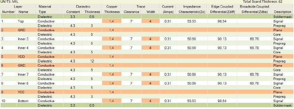
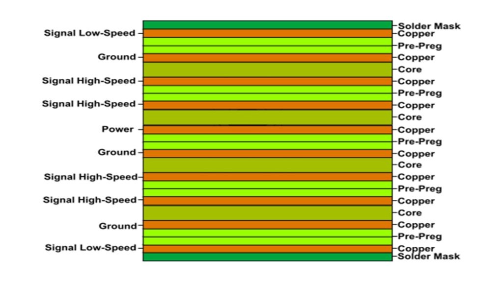
1. Standard Stackup Configuration
Example 8+2 HDI Structure:
Layer1: Signal (Top)
Layer2: Ground
Layer3: Signal (Stripline)
Layer4: Power
Layer5: Signal (Stripline)
Layer6: Core
Layer7: Signal (Stripline)
Layer8: Power
Layer9: Signal (Stripline)
Layer10: Signal (Bottom)
2. Impedance Control Techniques
- Differential Pair Specifications:
- 100Ω outer layers: 5/5mil width/spacing
- 90Ω inner layers: 4.5/8mil width/spacing
- Single-Ended Guidelines:
- 50Ω impedance: 8mil (outer), 6mil (inner) trace width
3. High-Density Interconnect Solutions
- Advanced Via Technologies:
- Laser microvias (0.1mm diameter)
- Mechanical buried vias (0.15mm)
- Staggered via structures
- Routing Density Enhancement:
- 8/8μm trace/space capability
- 45° diagonal routing
- Curved corner transitions
Free stackup optimization consulting available from the Topfast design team
In-Depth Analysis of 10-Layer PCB Manufacturing
1. Core Process Challenges
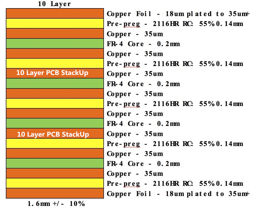
1. Precision Lamination Technology
- Critical Parameters:
- Vacuum level: ≤100Pa
- Temperature ramp rate: 2-3℃/min
- Pressure control: 15-20kg/cm²
- Alignment Accuracy:
- CCD+IR hybrid alignment system
- ≤25μm layer-to-layer registration
2. Microvia Technology Comparison
| Parameter | Mechanical Drilling | Laser Drilling | Plasma Etching |
|---|---|---|---|
| Min Hole Size | 0.15mm | 0.05mm | 0.03mm |
| Aspect Ratio | 10:1 | 15:1 | 20:1 |
| Hole Wall Quality | Ra≤35μm | Ra≤15μm | Ra≤8μm |
Topfast production lines combine German LPKF lasers with Japanese Hitachi mechanical drills
3. Surface Finish Selection
- High-Frequency: Immersion Silver+OSP (lowest loss)
- High-Reliability: ENEPIG (best corrosion resistance)
- Cost-Sensitive: Immersion Tin (optimal value)
2. Quality Verification System
- Electrical Testing
- Impedance (TDR method)
- Insertion loss (VNA up to 40GHz)
- Insulation resistance (1000VDC)
- Reliability Validation
- Thermal stress: 6×260℃ reflow cycles
- Environmental: 1000hrs 85℃/85%RH
- Mechanical: 3-point bend (strain≤0.3%)
- Production Monitoring
- SPC for critical parameters
- 100% AOI inspection
- Full-process traceability
Topfast Laboratory is a CNAS-certified facility that provides professional testing reports.
Application Case Studies
Case 1: 5G Base Station RF Board
- Design Features:
- Hybrid stackup: Rogers+FR4 combination
- Ultra-low loss: Df≤0.003@28GHz
- Tight impedance control: ±5% tolerance
Case 2: AI Server Motherboard
- Solutions:
- 16μm ultra-thin dielectrics
- Any-layer interconnect technology
- 3D EM simulation optimization
Case 3: Industrial Power Module
- Key Technologies:
- 2oz heavy copper design
- Enhanced thermal management
- High Tg material selection
More case details → Contact Topfast Technical Team


Related Posts