8-Layer PCB
As the “backbone” of electronic products, PCB technology must evolve in tandem to meet increasingly demanding requirements. With its superior multi-layer architecture and signal integrity advantages, the 8-layer PCB has become an indispensable key component in modern high-end electronic devices.
Table of Contents
Architectural advantages of 8-layer PCBs
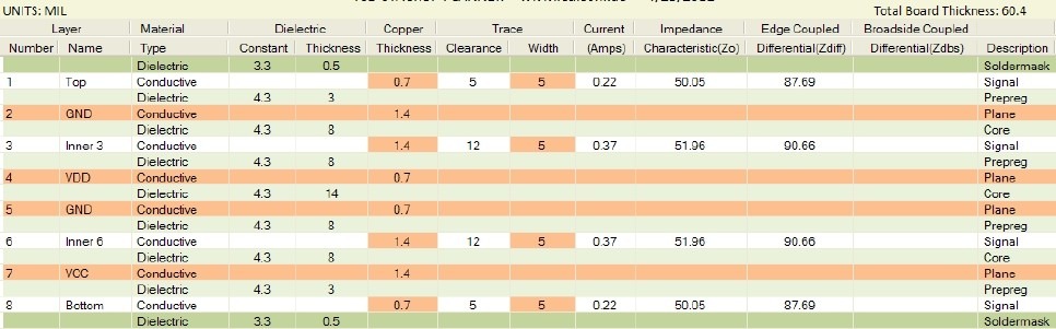
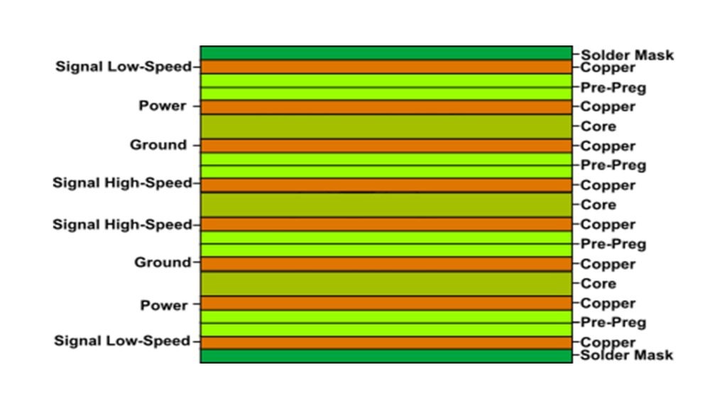
1. Precision Stack-Up Design
Our 8-layer PCBs adopt an industry-leading “2-4-2” symmetrical stack-up structure:
- Top and Bottom Layers: Signal layers (microstrip design)
- Layers 2 & 7: Ground planes (complete reference planes)
- Layers 3 & 6: Inner signal layers (stripline design)
- Layers 4 & 5: Power planes (split power domains)
This structure ensures:
✓ Excellent EMI shielding performance (15-20dB reduction in radiation)
✓ Impedance control accuracy within ±5%
✓ 30%+ improvement in crosstalk suppression
2. Signal Integrity Optimization
Key parameters for high-speed design:
- Supports 28Gbps+ high-speed signal transmission
- Insertion loss <0.5dB/inch @ @10GHz
- Delay skew controlled within ±10ps/inch
- Compatible with DDR4/DDR5 memory interfaces
Breakthrough Applications in Material Science
1. High-Performance Substrate Options
We offer multiple material solutions for different needs:
- Standard: FR-4 Tg170 (cost-effective solution)
- High-Frequency: Rogers 4350B (5G mmWave applications)
- High-Reliability: Megtron 6 (servers/data centers)
- Special Applications: Polyimide (aerospace)
2. Copper Foil Technology Innovation
Using Reverse Treat Foil (RTF) technology:
- Surface roughness reduced to 1.2μm
- 20% improvement in insertion loss
- 15% increase in peel strength
The Pursuit of Manufacturing Excellence
1. High-Precision Processing Capabilities
- Laser drilling: Minimum hole size 75μm
- Trace/space: 3/3mil (mass production capability)
- Layer-to-layer alignment accuracy: ±25μm
- Board thickness tolerance: ±8%
2. Advanced Surface Finishes
Optimal solutions for different applications:
- ENIG (standard digital circuits)
- ENEPIG (high-frequency/RF applications)
- Immersion silver (high-speed digital design)
- OSP (consumer electronics)
Typical Applications and Solutions
1. 5G Communication Equipment
- Base station AAU: Supports mmWave frequencies
- Optical modules: 56Gbps PAM4 signal transmission
- Small cells: High-density integration solutions
2. AI Hardware
- GPU accelerator cards: 16-layer stack design
- TPU modules: High-power-density thermal solutions
- Edge computing devices: Compact design
3. Automotive Electronics
- ADAS control units: Automotive-grade reliability
- Smart cockpits: Multi-display driving
- In-vehicle networks: High-speed bus design
Reliability Verification System
We have established a comprehensive quality assurance system:
- Design Phase: SI/PI simulation analysis
- Prototype Phase:
- Impedance testing (TDR)
- Thermal shock testing (-55℃~125℃, 1000 cycles)
- Highly Accelerated Life Test (HALT)
- Mass Production Phase:
- 100% electrical testing
- AOI full inspection
- Periodic reliability sampling
Customer Support Ecosystem
We provide full-range technical support:
- Design Consultation: From schematics to PCB layout guidance
- Simulation Services: HyperLynx/SIwave analysis
- Testing Services: Test boards and reports provided
- Rapid Prototyping: 5-day sample delivery
- Mass Production Support: Monthly capacity of 50,000㎡
“By choosing our 8-layer PCB solutions, you gain:
✓ Support from signal integrity experts
✓ Proven reliable design solutions
✓ Flexible production capacity
✓ Competitive lead times and costs”
Contact our technical consultants today for customized 8-layer PCB solutions tailored to your project!


Related Posts