A Comprehensive Analysis of PCB Warpage and Deformation
Table of Contents
1. What is PCB Warping?
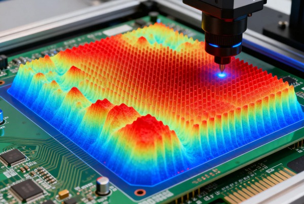
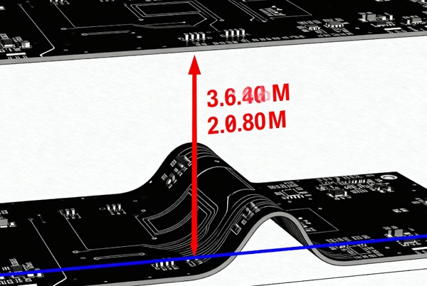
PCB warping refers to the shape change of printed circuit boards during production or use, resulting in the loss of original flatness. When a PCB is placed flat on a desktop, the warpage percentage is calculated by measuring the gap between the highest point and the desktop, divided by the board’s diagonal length.
Warpage Calculation Formula: Warpage = (Single Corner Warp Height / (PCB Diagonal Length × 2)) × 100%
PCB Warpage Standards
| Application Scenario | Allowable Warpage | Remarks |
|---|---|---|
| General Consumer Electronics | ≤0.75% | Basic IPC Standard Requirement |
| High-Precision SMT | ≤0.50% | Mobile phones, communication equipment, etc. |
| Ultra-High Precision Requirements | ≤0.30% | Military, medical, and other special fields |
| Plug-in Process Only | ≤1.50% | No surface mount components |

2. Serious Impacts of PCB Warping
2.1 Manufacturing Process
- Mounting Difficulties: On automated SMT lines, uneven PCBs cause positioning inaccuracies, preventing proper component insertion or mounting
- Equipment Damage: Severe warping may damage automatic insertion machines, causing production line downtime
- Welding Defects: Warping leads to uneven heat distribution at solder joints, causing issues like virtual soldering and tombstoning
2.2 Product Reliability
- Assembly Issues: Warped boards after soldering make it difficult to neatly trim component leads, preventing proper installation into chassis or sockets
- Long-term Risks: Stress concentration points are prone to circuit breakage under high-low temperature cycling environments
- Performance Degradation: Cases where automotive radar systems frequently failed after summer exposure due to excessive warpage
3. Main Causes of PCB Warping
3.1 Material Factors
- CTE Mismatch: Significant difference in thermal expansion coefficient between copper foil (17×10⁻⁶/℃) and FR-4 substrate (50-70×10⁻⁶/℃)
- Substrate Quality: Low Tg value, high moisture absorption, or incomplete curing reduces dimensional stability
- Material Asymmetry: Inconsistent core and PP board brands or thickness mismatches in multilayer boards
3.2 Design Issues
- Uneven Copper Distribution: Large copper areas on one side versus sparse circuits on the other, causing warping toward the copper-deficient side during heating
- Asymmetric Structure: Special dielectric layers or impedance requirements leading to unbalanced lamination structures
- Excessive Hollow Areas: Too many hollow areas in large boards, prone to bending after reflow soldering
- Excessive V-Cut Depth: Compromises structural integrity, with risk increasing when residual thickness ≤1/3 board thickness
3.3 Production Processes
Process-Induced Warping Analysis:
- Lamination Process: Improper temperature and pressure control, uneven resin curing
- Thermal Processing: Hot air leveling (250-265℃), solder mask baking (150℃), reflow soldering (230-260℃)
- Cooling Process: Excessive cooling speed, insufficient stress relief
- Mechanical Stress: Stacking, handling, and baking processes
3.4 Storage and Environment
- Humidity Effects: Copper-clad laminate moisture absorption and expansion, particularly significant for single-sided panels with larger absorption areas
- Storage Methods: Vertical storage or heavy compression causing mechanical deformation
- Temperature-Humidity Fluctuations: Exceeding standard ranges of 15-25℃/40-60%RH
4. PCB Warping Improvement and Prevention Measures
4.1 Material Selection Optimization
Substrate Selection Strategy Table:
| Application Scenario | Recommended Material | Characteristic Advantages | Warpage Improvement Effect |
|---|---|---|---|
| General Consumer Electronics | High Tg FR-4 (Tg≥170℃) | Good heat resistance | 30% better warpage resistance than ordinary materials |
| Automotive Electronics | Special FR-4 (Tg>180℃) | High temperature stability | Suitable for high-temperature engine compartment environments |
| High-Frequency Applications | Carbon fiber reinforced composites | CTE reducible to 8ppm/℃ | 50% reduction in thermal deformation |
| High Humidity Environments | PTFE composites | Water absorption ≤0.1% | Excellent moisture resistance |
4.2 Design Optimization Strategies
Copper Balance Design
- Symmetrical Layout: Control the copper area difference between A/B sides within 15%
- Grid-Based Copper Pouring: Change continuous copper to a grid pattern (line width/spacing ≥0.5mm), reducing thermal stress by 30%
- Hollow Area Treatment: Add balanced copper blocks or process edge copper pouring
Structural Design Essentials
- Interlayer Balance: Ensure symmetrical PP sheet distribution in multilayer boards, with consistent thickness between 1-2 and 5-6 layers
- Thickness Selection: Recommended thickness ≥1.6mm for SMT boards, warpage risk increases 3 times for boards below 0.8mm
- Panel Design: Use X-type panel structures to disperse stress, with proper V-Cut residual thickness control
4.3 Production Process Control
Lamination Process Optimization
Step Pressure Process Example:
- Penetration Stage: 5-10kg/cm² for complete resin flow
- Diffusion Stage: 20-25kg/cm² for optimal interlayer bonding
- Curing Stage: 30-35kg/cm² for complete curing
Temperature Control Profile:
- Heating Rate: Slow heating at 1℃/min
- Soaking Stage: Stepwise soaking at 130℃/150℃ for 10 minutes each
- Effect: 40% improvement in resin flow uniformity
Key Process Control Points
- Pre-cutting Baking: 150℃, 8±2 hours to remove moisture and release stress
- Prepreg Treatment: Distinguish warp and weft directions (warp direction shrinkage rate 0.2% lower than weft)
- Cooling Control: Use step cooling, pausing 5 minutes for every 10℃ drop
- Post Hot-Air Leveling: Natural cooling on marble slabs, avoiding rapid cooling
4.4 Storage and Transportation Management
- Environmental Control: 15-25℃, 40-60%RH, short-term fluctuations ≤10%RH/4 hours
- Stacking Methods: Horizontal stacking ≤30 sheets (≤20 for precision boards), avoid vertical storage
- Packaging Protection: Vacuum aluminum foil bags + silica gel desiccant (≥5g/㎡), cushioning material isolation
5. PCB Warping Repair Methods
5.1 In-Process Repair
- Roller Leveling: Immediate treatment of warped boards discovered during processes using roller leveling machines
- Hot Press Leveling: Use bow-shaped molds for baking and leveling near the substrate Tg temperature
5.2 Finished Board Repair
| Repair Method | Applicable Scenarios | Effectiveness | Risks |
|---|---|---|---|
| Cold Press Leveling | Slight Warping | Average | Prone to Rebound |
| Hot Press Leveling | Moderate Warping | Good | Possible Discoloration |
| Bow Mold Hot Press | Various Warping Conditions | Best | Temperature/Time Control Required |
Bow Mold Hot Press Steps:
- Place the warped PCB with the curved surface facing the mold surface
- Adjust fixture screws to deform the PCB in the opposite direction
- Place in oven and heat near the substrate Tg temperature
- Maintain for a sufficient time for complete stress relaxation
- Remove from mold after cooling and stabilization
6. Detection and Quality Control
PCB Warpage Detection Method Comparison
| Detection Method | Precision | Speed | Cost | Applicable Scenarios |
|---|---|---|---|---|
| Visual Inspection | Low | Fast | Low | Preliminary Screening |
| Ruler/Feeler Gauge | Medium | Medium | Low | Routine Inspection |
| Laser Scanning | High | Fast | High | Mass Production |
| AOI System | High | Medium | High | High-Precision Detection |
Practical Quality Control Techniques
- Incoming Inspection: Use ruler + feeler gauge to measure gaps at four corners and midpoint of long edges, alert if exceeding 0.3mm
- Pre-soldering: Preheating is especially necessary for thick copper boards to release stress
- Regular Monitoring: Check copper foil oxidation for storage exceeding 6 months (scrap if color difference ΔE>5)
Summary
PCB warping is a critical factor affecting electronic product quality. Through multi-dimensional measures including material selection, design optimization, process control, and storage management, warpage can be effectively controlled within required limits. For existing warping issues, appropriate repair methods can also recover losses. Controlling PCB warpage is not only a technical issue but also a comprehensive reflection of cost and quality management, requiring collaborative efforts from design, production, and quality departments.


Related Posts