Table of Contents
Substrate Material: Standard FR-4 vs. Advanced Laminates
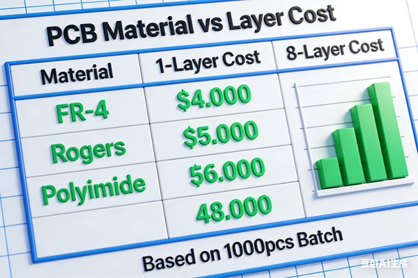
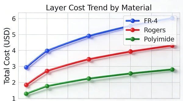
The base material is the largest cost driver. While standard FR-4 is economical for most consumer goods, high-speed or high-power designs require specialized materials.
- Cost Impact: Upgrading from FR-4 to low-loss materials (like Megtron 6) can increase material costs by 300%-500%.
- Pro Tip: Understanding what a PCB design requirement is early helps avoid over-speccing materials.
Layer Count and Sequential Lamination
Increasing the number of layers doesn’t just add material; it adds processing time and complexity.
- Standard Multi-layer: A 4-layer board is the “sweet spot” for cost vs. performance.
- HDI Impact: If your design requires HDI PCB manufacturing, the cost rises due to laser drilling and sequential lamination cycles. Refer to our Ultimate Guide to PCB Stack-up Design to optimize your layer usage.
Copper Weight and Specialized Features
Heavy copper (e.g., 3oz or 4oz) for power electronics increases cost due to longer etching times and additional raw copper usage.
- Design Strategy: Use PCB design optimization strategies to manage thermal loads rather than simply increasing copper thickness everywhere.
How-to: 5 Steps to Reduce PCB Manufacturing Costs
- Standardize Your Panel Usage
Design board dimensions to maximize the use of standard production panels, reducing waste.
- Optimize Layer Count
Only move to higher layer counts (e.g., from 6 to 8) if signal integrity cannot be maintained otherwise.
- Minimize Unique Via Types
Use through-hole vias instead of blind or buried vias where possible to avoid the complex HDI manufacturing process.
- Simplify Component Selection
Use standard SMD electronic components
to lower the complexity and cost of the PCBA processing flow. - Run a DFM Check
Identify high-cost features (like extremely small trace widths) before sending files to the factory.
Material & Layer Cost FAQ
A: No. Typically, moving from 4 to 6 layers increases the price by 30%-50%, not 100%, as the setup and testing costs remain similar.
A: Only for very short traces. For long signal paths, FR-4’s high Df (Dissipation Factor) causes signal loss, requiring advanced optimization strategies.
A: Microvias require laser drilling, which is more expensive than mechanical drilling. They are essential for HDI PCBs but should be avoided in low-cost standard designs.
A: The material cost difference is negligible now, but the PCBA processing requires higher reflow temperatures, which may require higher-Tg substrates.
A: Standard green is the cheapest. Specialized colors like matte black or purple can add to the lead time and cost due to additional machine cleanup.
Conclusion
PCB material and layer choices are critical levers for controlling manufacturing cost. By selecting appropriate substrates, optimizing layer count, and balancing copper thickness, engineers can produce high-quality, cost-effective PCBs.Choosing the right materials allows engineers to reduce PCB cost without sacrificing reliability or manufacturability
Early design decisions combined with DFM review and manufacturer guidance are key to achieving maximum cost efficiency without compromising reliability.
Related Reading