Minimum line width and line spacing for PCB
Table of Contents
What are PCB trace width and trace spacing?
In printed circuit board (PCB) design, trace width and trace spacing are two fundamental yet critical parameters:
- Trace Width: The width of the conductive copper foil, which determines current-carrying capacity and temperature rise.
- Trace Spacing: The distance between adjacent traces, affecting signal isolation and short-circuit risks.
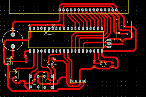
1. Industry Standard Minimum Trace Width and Spacing
1.1 Conventional Process Capabilities
- Mainstream Manufacturers: Over 80% can stably produce designs with 6 mil/6 mil (0.15 mm/0.15 mm) at lower costs.
- High-Precision Manufacturers: 70% support 4 mil/4 mil (0.1 mm/0.1 mm), suitable for most high-density designs.
1.2 Advanced Processes (HDI)
- Laser Drilling Microvia Technology: Supports 2 mil/2 mil (0.05 mm/0.05 mm), used in ultra-thin, high-density applications like smartphones and RF modules, but costs increase significantly.
1.3 Extreme Challenges
- 3.5 mil/3.5 mil (0.09 mm/0.09 mm) is limited to a few manufacturers and requires strict yield testing.
2. Four Key Factors Influencing Trace Width/Spacing Selection
2.1 Current Carrying Capacity and Temperature Rise
- Formula Reference: According to the IPC-2221 standard, trace width must meet current requirements. For example, with 1 oz copper thickness, a 1 A current requires at least 40 mil (1 mm) trace width (for a 10°C temperature rise).
- Tool Assistance: Use online PCB trace width calculators (e.g., Saturn PCB Toolkit) by inputting current, copper thickness, and temperature rise limits to quickly obtain recommended values.
2.2 Signal Integrity
- High-Speed Signals: Require impedance matching, where trace width relates to dielectric layer thickness and permittivity. For example, a 50 Ω microstrip line on an FR4 board typically has a trace width of 8–12 mil.
- Differential Pairs: Maintain equal width and spacing (e.g., 5 mil/5 mil) to reduce crosstalk.
2.3 Manufacturing Process and Cost
- Cost Threshold: When trace width/spacing < 5 mil, prices may double (due to lower yields and laser process requirements).
- Copper Thickness Selection: Outer layers commonly use 1 oz (35 μm), inner layers 0.5 oz; for high-current scenarios, 2 oz copper thickness can be used but requires wider traces.
2.4 Layout Density and BGA Design
- BGA Escape Routing: For 1 mm pitch BGAs, use 6 mil/6 mil if routing one trace between two pins; use 4 mil/4 mil if routing two traces.
- Avoid Bottlenecks: Plan trace widths in high-density areas early to avoid rework later.
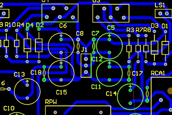
3. PCB Design Optimization Strategies
3.1 Layer Strategy
- Power Layers: Use wide traces or copper pours (e.g., 50 mil+) to reduce impedance and heat generation.
- Signal Layers: Prioritize high-frequency signals on inner layers (stripline structure) to minimize radiation interference.
3.2 Avoid Common Mistakes
- Sharp-Angle Traces: Replace with 45° or curved corners to reduce impedance discontinuities.
- Ignoring Manufacturer Feedback: Confirm process capability documents (e.g., minimum aperture, trace width tolerances) before finalizing designs.
3.3 Cost Balancing
- Prioritize Relaxing Non-Critical Signals: Use 8–10 mil trace widths for general I/O signals to save space for critical paths.
Optimizing PCB trace width and spacing requires balancing electrical performance, process limitations, and cost. 4 mil/4 mil is the sweet spot for most high-density designs, while 2 mil/2 mil is reserved for high-end HDI applications. Early-stage design should use calculation tools to verify current requirements and communicate with manufacturers to ensure producibility.
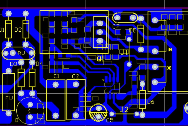
4. PCB Design Spacing Specifications
1. Traces
- Min. Width: 5mil (0.127mm)
- Min. Spacing: 5mil (0.127mm)
- Trace to Board Edge: ≥0.3mm (20mil)
2. Vias
- Min. Hole Size: 0.3mm (12mil)
- Pad Ring Width: ≥6mil (0.153mm)
- Via-to-Via Spacing: ≥6mil (edge-to-edge)
- Via to Board Edge: ≥0.508mm (20mil)
3. PTH Pads (Plated Through-Holes)
- Min. Hole Size: ≥0.2mm larger than component lead
- Pad Ring Width: ≥0.2mm (8mil)
- Hole-to-Hole Spacing: ≥0.3mm (edge-to-edge)
- Pad to Board Edge: ≥0.508mm (20mil)
4. Solder Mask
- PTH/SMD Opening: ≥0.1mm (4mil) clearance
5. Silkscreen (Text)
- Min. Line Width: 6mil (0.153mm)
- Min. Height: 32mil (0.811mm)
6. Non-Plated Slots
- Min. Spacing: ≥1.6mm
7. Panelization
- Spacing (1.6mm board): ≥1.6mm
- V-Cut/No-Spacing: ~0.5mm
- Process Edge: ≥5mm





Related Posts