PCB Assembly Technology Overview
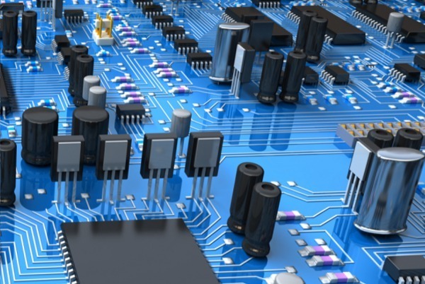
Printed circuit board (PCB) assembly is the process of mounting electronic components onto a PCB and forming an electrical connection, which is the core link in the manufacturing of modern electronic products. With the development of electronic products in the direction of miniaturization and high performance, PCB assembly technology is also evolving. Currently, the mainstream PCB assembly technology mainly includes through-hole mounting technology (THT), surface mounting technology (SMT), hybrid mounting technology, as well as manual and mechanical installation, and other forms.
PCB assembly is not only a simple component fixed on the substrate, but also a complex process involving materials science, precision machinery, thermodynamics and electronics, and another interdisciplinary processes. The selection of appropriate assembly technology directly affects product reliability, production costs, and market competitiveness. According to statistics, the global PCB assembly market size in 2023 has reached about 80 billion U.S. dollars, and is expected to grow to 120 billion U.S. dollars by 2028, with a compound annual growth rate of about 6.5%.
Through-Hole Mounting Technology (THT) is one of the earliest PCB assembly methods and still plays an important role in specific areas. The basic principle of THT technology is to insert the pins of components into pre-drilled through-holes on the PCB, and then solder them in place on the other side of the PCB.
THT Technology Features
THT technology has several notable features: first, it forms a very strong mechanical connection that can withstand large physical and thermal stresses, which makes THT particularly suitable for application scenarios that require high reliability, such as aerospace, military equipment, and industrial control systems. Secondly, THT components usually have large pin spacing, which facilitates manual operation and maintenance. According to IPC standards, common THT components have a pin pitch of 2.54mm (0.1 inches), while some high-power components may have a pitch of 5.08mm or more.
THT Process Flow
A typical THT process flow consists of the following steps:
- Component Insertion: Manually or automatically align the component pins with the PCB via holes and insert them
- Pin Bending: To prevent the component from falling out, the pins are usually bent slightly outwards
- Wave soldering: PCB passes through a wave soldering machine, molten solder contacts all pins from the bottom to form a solder joint.
- Pin Trimming: Use a special tool to cut off excessively long pins.
- Cleaning and Inspection: Flux residue is removed, and visual or automated optical inspection is performed.
THT Technology Advantages and Limitations
The main advantage of THT technology is its excellent mechanical strength and reliability. According to research data, the failure rate of THT solder joints in vibration environments is approximately 30-40% lower than that of SMT solder joints. In addition, THT technology has fewer restrictions on component size and is suitable for high-power, high-voltage components such as electrolytic capacitors, transformers, and high-power resistors.
However, THT technology also has obvious limitations: lower production efficiency, modern high-speed THT plug-in machine speed of about 20,000-30,000 components per hour, much lower than the SMT mounter; PCB needs to drill a large number of through-holes, increasing the cost of board production; can not achieve high-density assembly, limiting the development of miniaturization of electronic products.
THT Application Scenarios
Although SMT technology has become mainstream, THT still maintains an important position in the following fields:
- Military and aerospace electronic equipment with high reliability requirements
- High-power power supplies and power electronics
- Connector assemblies that require frequent plugging and unplugging
- Educational experimentation and prototyping
- Electronic equipment used in special environments (e.g., high temperature, high humidity environments)
Surface Mount Technology (SMT) is the mainstream technology for PCB assembly today, revolutionizing the face of electronics manufacturing.SMT technology directly mounts components on pads on the surface of the PCB and realizes electrical and mechanical connections through the reflow process.
SMT Technology Revolution
The emergence of SMT technology has brought about three major revolutions** in the electronics manufacturing industry: first, the size revolution, SMT component size can be 60-70% smaller than THT components, so that cell phones, smart watches and other ultra-portable devices become possible; second, the efficiency revolution, modern SMT production lines can be mounted more than 100,000 components per hour; and lastly, the cost revolution, SMT reduces PCB drilling process, reduces material consumption. material consumption.
SMT key process steps
- Solder Paste Printing: Stainless steel stencils are used to accurately print solder paste onto PCB pads. Solder paste is a mixture of tiny solder particles (usually Sn96.5/Ag3.0/Cu0.5 alloy) and flux, whose viscosity and metal content need to be strictly controlled. Studies have shown that the quality of solder paste printing directly affects about 70% of the SMT soldering defects.
- Component placement: High-speed mounter through the vacuum nozzle will SMD components accurately on the solder paste. The positioning accuracy of modern placement machines can reach ±25μm, and the maximum speed exceeds 150,000 components per hour. 0201 (0.6mm × 0.3mm) or even smaller size components have become mainstream.
- Reflow Soldering: PCBs pass through the reflow oven through four temperature zones: preheating, wetting, reflow, and cooling. Typical lead-free solder peak temperature of about 240-250 ℃, time control in 60-90 seconds. Precise control of the temperature profile is essential to avoid defects such as “tombstone effect” and “solder balls”.
Advantages of SMT technology
The core advantages of SMT technology are reflected in:
- High-density integration: BGA and CSP packages with a pitch of 0.4mm and below can be realized.
- **Excellent high-frequency characteristics **: SMD components with small parasitic parameters, suitable for high-frequency circuits
- High degree of automation: fully automated production can be realized from printing to testing
- Double-sided assembly capability: full utilization of PCB space, increase assembly density
Challenges facing SMT
Despite the obvious advantages, SMT technology faces some challenges:
- Miniaturization brings increased difficulty in detection. A 01005 (0.4mm x 0.2mm) component detection requires 3D SPI equipment
- Higher temperatures of lead-free soldering put higher requirements on components and PCB materials
- Ultra-fine pitch soldering reliability issues, such as cracked solder joints, false soldering, etc.
- Rework is difficult, especially for bottom-filled BGA components.
SMT Technology Trends
SMT technology continues to evolve, and the main development directions include:
- Ultra-fine pitch technology: to cope with CSP and POP packages with a pitch of 0.3mm or less.
- 3D SMT technology: three-dimensional integration through stacking
- Low temperature SMT process: adapting to flexible substrates and heat-sensitive components
- Smart SMT line: combining AI and IoT technologies for predictive maintenance and quality control
Hybrid mounting technology fully analyzed
Hybrid mounting technology is an organic combination of THT and SMT technology, which is widely used in modern complex electronic products. According to statistics, about 35% of industrial control boards and 20% of automotive electronic boards use hybrid mounting technology.
The need for hybrid mounting
The fundamental reason for the birth of hybrid mounting technology lies in the diversification of the functions of electronic products. Take a typical industrial controller as an example, it requires both SMT technology to realize high-density digital circuits and THT technology to install high-power relays and robust connectors. Mixed use cases in medical devices show that the SMT portion takes up 70-80% of the board area, but the THT portion takes on critical signal interface and power management functions.
Mixed mount process sequence
The process sequence for mixed mounting is critical to the quality of the finished product, and there are two common routes:
- Complete SMT face printing, placement, and reflow
- Flip PCB for THT component insertion
- Wave soldering THT surface (need to protect the SMT components that have been soldered)
- Manual soldering of SMT components that cannot withstand wave soldering
- Insert the THT components first, but do not solder them yet
- Perform SMT face printing, placement, and reflow.
- Selective wave soldering or manual soldering at the end.
Studies have shown that the combined yield of the SMT-first route is about 5-8% higher than the THT-first route, but requires more complex process design and fixture protection.
Hybrid Mount Design Essentials
A successful hybrid mount design requires consideration of several key factors:
- Component layout strategy: THT components should be centrally located to facilitate subsequent soldering processes
- Thermal management design: THT soldering needs to protect neighboring SMT components from thermal damage.
- Process compatibility: Select THT components that can withstand secondary reflow temperatures
- Balance of cost: Evaluate which THT components can be replaced with SMT versions to reduce cost.
Typical applications for hybrid installations
Hybrid mounting technology excels in the following areas:
- Automotive electronics: engine control units (ECUs) combining SMT microcontrollers and THT power devices
- Industrial equipment: SMT logic circuits and THT relays/connectors in PLC modules
- Medical Electronics: SMT signal processing circuits with THT high voltage isolation components
- Aerospace: SMT digital systems with hardened THT interface components
Manual vs. Mechanical Mounting Comparative Analysis
In addition to mainstream THT and SMT technologies, Manual mounting and Mechanical mounting are also important complementary means of PCB assembly, each applicable to different production scenarios.
Manual mounting technology
Manual mounting is the most primitive PCB assembly method, and still plays a role in specific occasions. Manual soldering technology can be divided into two categories: basic manual soldering and precision manual soldering.
Basic hand soldering uses an ordinary soldering iron and is suitable for:
- Prototyping and R&D stages
- Small batch production (usually <100pcs/month)
- Assembly of large-sized components
- Field repairs and modifications
Precision hand soldering requires a microscope and a microfine soldering iron tip for:
- Rework of 0402 and below size components
- Reballing of BGA and QFN packages
- High reliability soldering of aerospace-grade products
- Specialized handling of shaped components
The primary advantages of manual mounting are flexibility and low cost, but its limitations are also evident: poor consistency (studies have shown that the defect rate of manual solder joints is 3-5 times higher than that of automated soldering), inefficiency (skilled laborers complete approximately 200-300 solder joints per hour), and dependence on operator skill.
Mechanical mounting technology
Mechanical mounting represents the highly automated direction of PCB assembly, mainly including:
- Automatic Inserter (AI): inserts THT components at high speeds up to 45,000 components per hour
- Selective Wave Soldering: precise control of the soldering area to minimize thermal shock
- Automatic Optical Inspection (AOI): realizes 100% solder joint quality inspection
- Robotic assembly cell: flexible handling of shaped components
The core value of mechanical mounting lies in:
- Ultra-high efficiency: one fully automated SMT line can produce thousands of complex PCBs per day
- Excellent consistency: CPK values up to 1.67 or more
- Traceability: Full data logging for easy quality analysis
- Long-term cost advantage: Although the initial investment is high, the cost per piece is significantly lower at high volumes.
How to choose the right PCB assembly technique
The following Key Factors should be considered when choosing between manual or mechanical installation:
| Considerations | Manual Installation Advantage Scenarios | Mechanical Installation Advantage Scenarios |
|---|
| Batch Size | <100pcs/month | >1000pcs/month |
| Component Type | Shaped/Oversized Components | Standard SMD/THT Components |
| Quality Requirements | General Commercial Grade | High Reliability/Automotive Medical Grade |
| Investment Budget | Limited (<$50k) | Sufficient (>$500k) |
| Product Life Cycle | Short (≤ 1 year) | Long (≥ 3 years) |
| Frequency of change | High (weekly) | Low (quarterly) |
Conclusion
PCB assembly technology, as the core link of electronic manufacturing, has developed from a pure production process to a comprehensive technology system integrating material science, precision machinery, thermodynamics, and intelligent algorithms. Through in-depth analysis of mainstream technologies such as THT, SMT, and hybrid mounting, we can see the development trajectory and future direction of electronics manufacturing technology.
Technology integration will become the main theme of future development, the traditional boundaries will gradually blur. For example, the new “half-through-hole” technology combines the reliability of THT and the high-density advantages of SMT; 3D printing electronics technology may revolutionize the existing assembly model. According to Prismark’s forecast, by 2028, SMT will account for 85% of the global PCB assembly market, but THT will maintain a 10-15% share in specific areas, and hybrid mounting technologies will continue to grow in complex industrial products.
Sustainability Pressure to drive technology innovation.
- Halogen-free lead-free assembly processes
- Low-temperature, energy-efficient production technologies
- Recyclable design solutions
- Biodegradable electronic materials
Over the next five years, green assembly technologies are likely to become a basic requirement for market access.