PCB Design Optimization Strategies
Table of Contents
PCB Design Spacing Guidelines for Optimal Manufacturing
1. Trace Design Specifications
Minimum Trace Width: 5mil (0.127mm)
- Absolute lower limit for production
- Recommended design width: 10mil+
- Wider traces improve:
- Manufacturability
- Current capacity
- Thermal performance
Trace Spacing: 5mil (0.127mm) minimum
- Line-to-line and line-to-pad clearance
- Design recommendation: 10mil+ spacing
- Critical for:
- High voltage applications
- Signal integrity
- Manufacturing yield
Board Edge Clearance: 0.3mm (20mil)
- Prevents copper peeling during routing
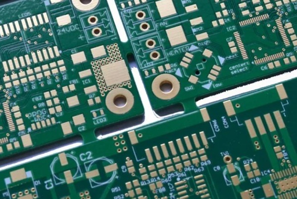
2. Via Design Requirements
Hole Size: 0.3mm (12mil) minimum
- Microvias require laser drilling (additional cost)
Pad Annular Ring: 6mil (0.153mm) minimum
- Recommended: 8mil+
- Ensures reliable plating
Via-to-Via Spacing: 6mil edge-to-edge
- 8mil+ recommended for high reliability
Board Edge Clearance: 0.508mm (20mil)
3. PTH (Plated Through-Hole) Specifications
Hole Size Tolerance
- Minimum +0.2mm over component lead
- Example: 0.6mm lead → 0.8mm hole
Pad Ring Width: 0.2mm (8mil) minimum
- Larger rings improve reliability
Hole-to-Hole Spacing: 0.3mm minimum
4. Solder Mask Considerations
Clearance: 0.1mm (4mil) minimum
- Applies to both PTH and SMD pads
- Prevents solder bridging
5. Silkscreen Legibility
Minimum Text:
- Width: 0.153mm (6mil)
- Height: 0.811mm (32mil)
- Optimal ratio: 1:5 (width: height)
6. Non-Plated Slots
Minimum Spacing: 1.6mm
- Reduces milling complexity
7. Panelization Guidelines
Spacing Options:
- Gapped: ≥1.6mm (matches board thickness)
- V-cut: 0.5mm
- Process borders: ≥5mm
5 Common PCB Design Challenges & Solutions
- 1. Insufficient Trace Width for Current
- Problem: Overheating traces
- Solution: Use IPC-2152 calculators
- 2. Via-in-Pad Without Proper Filling
- Problem: Solder wicking
- Solution: Specify via fill or tenting
- 3. Tight Component Spacing
- Problem: Assembly difficulties
- Solution: Follow DFM guidelines
- 4. Inadequate Thermal Relief
- Problem: Poor soldering
- Solution: Add thermal spokes
- 5. Incorrect Layer Stackup
- Problem: Impedance mismatch
- Solution: Simulate before production
PCB Design Considerations
1. Exceed minimum spacing requirements as much as possible.
2. Communicate with the manufacturer.
3. Strictly enforce design rule checks (DRC).
4. Consider panelization requirements during layout.
5. Allow for dimensional tolerances.


Related Posts