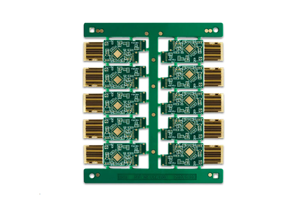
PCB Layer Selection Strategy
In electronic product development, the choice of PCB layer count is a critical decision that affects the success or failure of a project. According to Topfast’s big data analysis statistics, approximately 38% of PCB design rework is due to improper initial layer planning. How to make the best choice based on project requirements is very important.

Table of Contents
Comparison of PCB layers from 1 to 16+ layers
1. Single-Layer PCBs
Structural Anatomy
- Basic construction: FR-4 substrate + single-side copper foil (35/70μm)
- Typical thickness: 1.6mm (customizable 0.8-2.4mm)
- Surface finish: Most commonly HASL (lead/lead-free)
Key Advantages
Lowest cost (40-50% cheaper than double-layer)
24-hour rapid prototyping is widely available
Easiest for manual soldering/repair
Performance Limitations
Routing density <0.3m/cm² (limited by jumpers)
Poor signal integrity (ΔIL>3dB/inch@1GHz)
No EMI protection (>60% radiation risk)
Classic Applications
- Consumer electronics: Scales, remotes
- Lighting systems: LED drivers
- Basic industrial controls: Relay modules
2. Double-Layer PCBs
Technical Evolution
- Via types: PTH (plated) vs NPTH (mechanical)
- Modern capabilities: Supports 4/4mil trace/space
- Impedance control: ±15% tolerance achievable
Design Benefits
2-3× higher routing density (vs single-layer)
Basic impedance control (microstrip structure)
Moderate EMC performance (20dB improvement over single-layer)
Cost Analysis
- Material cost: +50% (vs single-layer)
- Prototype lead time: +1 working day
- Complex designs: May require jumper resistors
Typical Applications
- Automotive electronics: ECU control units
- IoT devices: Wi-Fi endpoints
- Industrial controls: PLC I/O modules
Consult a professional engineer to make your design simpler
3. Four-Layer PCBs
Optimal Stackup Structure
- Top (signal)
- GND (solid plane)
- Power (split plane)
- Bottom (signal)
Performance Breakthroughs
40% lower crosstalk (vs double-layer)
Power impedance <100mΩ (with proper decoupling)
Supports high-speed buses like DDR3-1600
Cost Impact
- Material cost: +80% (vs double-layer)
- Design complexity: Requires SI simulation
- Production lead time: +2-3 days
High-End Applications
- Medical devices: Ultrasound probes
- Industrial cameras: 2MP processing
- Automotive ADAS: Radar modules
4. Six-Layer+ PCBs
Typical Configurations
6-layer: S-G-S-P-S-G (best EMI)
8-layer: S-G-S-P-P-S-G-S
12-layer: G-S-S-G-P-P-G-S-S-G-P
Technical Advantages
Supports 10Gbps+ high-speed signals
Power integrity (PDN impedance <30mΩ)
300% more routing channels (vs 4-layer)
Cost Considerations
- 6-layer: 35-45% more than 4-layer
- 8-layer: 50-60% more than 6-layer
- 12-layer+: Significant yield impact
Cutting-Edge Applications
- 5G base stations: mmWave antenna arrays
- AI accelerators: HBM memory interconnects
- Autonomous driving: Domain controllers
PCB Layer Selection Decision Tree
“3 Steps to Determine Your Ideal PCB Layers:”
- Signal Analysis
- High-speed signal count (>100MHz)
- Differential pair density (pairs/cm²)
- Special impedance requirements (e.g., 90Ω USB)
2. Power Evaluation
- Voltage domain count
- Maximum current needs (A/mm)
- Noise-sensitive circuit percentage
3. Cost Tradeoffs
- Budget constraints ($/cm²)
- Production volume (K units/month)
- Iteration risk tolerance
Most modern electronics optimally balance performance/cost with 4-6 layers!
Five Golden Rules of PCB Layer Design
- 3:1 Rule: 1 ground plane per 3 signal layers
Exception: RF circuits need a 1:1 reference - 20H Principle: Power plane inset 20× dielectric thickness
Modern approach: Use edge guard rings - Symmetry Law: Prevent warping (balanced copper distribution)
Key parameter: ΔCu<15% across layers - No Cross-Split: Never route high-speed over plane splits
Solution: Use stitching capacitors - Cost Optimization Formula:
Ideal layers = ceil(Total routing needs / Layer efficiency)Experience values: 4-layer ≈55%, 6-layer ≈70% utilization
Consult us for the best advice
PCB Layer Technology
1. Heterogeneous Integration
- Embedded component PCBs (EDC)
- Silicon interposer 2.5D integration
- 3D-printed multilayer structures
2. Material Innovations
- Ultra-low loss substrates (Dk<3.0)
- Thermal dielectrics (5W/mK+)
- Recyclable laminate materials
3. Design Revolution
- AI-powered layer optimization
- Quantum computing stackups
- Neuromorphic routing architectures
Industry Forecast: By 2026, 20+ layer PCBs will occupy 35% of high-end markets, but 4-8 layers remain mainstream (>60%)
Frequently Asked Questions
Q: When should I increase PCB layers?
A: Consider more layers when:
- >30% nets require long detours
- Power noise causes instability
- EMC tests repeatedly fail
Q: Can 4-layer replace 6-layer designs?
A: Possible with:
HDI microvias
2 signal + 2 mixed planes
Buried capacitance
But sacrifices ~20% performance margin
Q: Typical lead time for multilayer PCBs?
A: Standard delivery:
- 4-layer: 5-7 days
- 6-layer: 7-10 days
- 8-layer+: 10-14 days
(Expedited services reduced by 30-50%)

Reasonable selection of PCB layer count
- Performance Needs > Theoretical specs: Real tests beat simulations
- Cost Control requires lifecycle analysis: Include rework risks
- Supply Chain alignment: Avoid over-engineering
“The best PCB layer choice meets current needs while allowing future upgrades!”


Related Posts