SMT Patch Processing Terminals
In the field of modern electronics manufacturing, SMT (surface mount technology) chip processing has become a core process in circuit board assembly. As a key component in circuit connections, terminals play a crucial role in SMT chip processing.
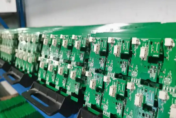
Table of Contents
The Core Role of Terminals in SMT Surface Mount Assembly
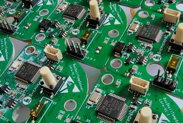
Terminals serve as critical interfaces in electronic circuits, enabling secure electrical connections between components, circuits, or devices on a printed circuit board (PCB). In surface-mount technology (SMT) assembly, terminals are typically designed as compact, lightweight surface-mount devices (SMDs) and are precisely soldered onto PCB pads using automated processes. Compared to through-hole technology (THT), SMT-mounted terminals offer superior space efficiency, higher component density, and compatibility with modern electronics’ miniaturization trends.
Key Functions and Advantages
- Electrical Connectivity: Terminals establish reliable conductive pathways between components, ensuring uninterrupted signal and power transmission.
- Miniaturization: SMT terminals enable smaller PCB designs, critical for compact devices like smartphones, wearables, and IoT modules.
- High-Density Assembly: Their low-profile design supports advanced PCB layouts with tightly spaced components.
- Process Efficiency: Automated SMT placement and reflow soldering enhance production speed and consistency.
Impact on Product Performance
- Signal Integrity: Properly soldered terminals minimize impedance and signal loss, vital for high-frequency applications (e.g., 5G devices).
- Mechanical Stability: Solder joint quality directly affects resistance to vibration and thermal stress (e.g., in automotive electronics).
- Reliability: Defects like tombstoning or cold joints can lead to field failures, underscoring the need for precise process control.
Diverse Terminal Types and Their Characteristics
The diverse application scenarios in the field of electronics manufacturing have given rise to various types of SMT (Surface Mount Technology) terminals, each designed to meet specific connection requirements:
1. Wire-to-Board Terminals
- Characteristics:
- Designed for connecting wires to PCBs, commonly used in power distribution and signal transmission circuits.
- Provides robust mechanical connections for long-term electrical stability.
- Applications:
- Power supplies, industrial control boards (e.g., PLC modules).
- Example Models: Phoenix CONTACT PT series.
2. Plug-in Terminals
- Characteristics:
- Allows easy connection and disconnection, ideal for modular devices requiring frequent maintenance.
- Optimized contact structure ensures durability after repeated mating cycles.
- Applications:
- Replaceable modules (e.g., server backplanes, LED arrays).
- Test fixtures (e.g., probe interfaces).
3. Spring Terminals
- Characteristics:
- Uses precision spring mechanisms for consistent contact pressure.
- Resistant to vibration and mechanical shock, ideal for harsh environments.
- Applications:
- Automotive electronics (ECUs, sensors, compliant with ISO 16750).
- Industrial control systems.
- Example Brands: WAGO CAGE CLAMP® series.
4. Screw Terminals
- Characteristics:
- High mechanical strength due to threaded fastening.
- Supports high-current applications (up to 200A).
- Applications:
- Power transmission (e.g., inverters, transformers).
- Motor drives (e.g., VFD outputs).
5. Special-Environment Terminals
5.1 Waterproof Terminals (IP67/IP68)
- Key Features:
- Sealed with silicone gaskets or potting compounds.
- Corrosion-resistant (e.g., EV charging connectors).
- Applications: Outdoor LED lighting, electric vehicle charging ports.
5.2 High-Temperature Terminals (150°C+)
- Materials:
- Housing: PPS, LCP engineering plastics.
- Contacts: Nickel or nickel alloy plating.
- Applications: Engine bay sensors, aerospace electronics.
5.3 High-Frequency Terminals (RF/High-Speed Signals)
- Characteristics:
- Impedance-matched (e.g., 50Ω/75Ω).
- Shielded to minimize crosstalk (e.g., SMA coaxial terminals).
- Applications: 5G base stations, high-speed data interfaces (USB4.0/HDMI 2.1).
Terminal Process Requirements
In the SMT assembly process, the quality of terminal soldering directly impacts the performance and reliability of the final product, so strict control of each process step is essential:
Pad Design
It is the first step in ensuring good soldering results. The size, shape, and position of the pads must precisely match the terminals, providing sufficient soldering area to ensure connection strength while avoiding excessive size that could cause soldering defects.
Solder Paste Printing Process
This process has a decisive impact on soldering quality. The thickness, quantity, and positional accuracy of the solder paste must be strictly controlled. Modern solder paste printers typically feature optical positioning and 3D detection capabilities to ensure printing quality.
Component placement process
requires extremely high positioning accuracy, especially for multi-pin or fine-pitch terminals. High-precision placement machines typically use visual alignment systems to achieve micron-level positioning accuracy. Placement pressure also needs to be optimized to ensure good contact between the terminal and solder paste while avoiding excessive pressure that could damage the component or PCB.
Reflow soldering
It is one of the most critical stages in the entire process. Precise temperature curves must be designed based on solder paste characteristics and the thermal capacity of terminals/PCBs to ensure adequate soldering while avoiding thermal damage.
Inspection and Testing
Serves as the final quality assurance checkpoint. Automatic optical inspection (AOI) can detect soldering appearance defects, while in-circuit testing (ICT) or functional testing verifies electrical connection performance. For high-reliability applications, more in-depth inspections such as X-ray inspection or cross-section analysis may also be required.
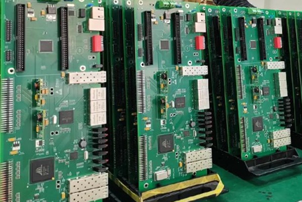
Application Areas
1. Consumer Electronics
In smartphones, tablets, smart TVs, and other devices, miniaturized SMT terminals connect various functional modules, ensuring efficient signal transmission. These terminals demand high precision and stability to meet the stringent reliability requirements of consumer electronics.
2. Industrial Control Systems
Terminals play a crucial role in connecting PLCs, sensors, and actuators in harsh industrial environments. They must offer:
- Strong anti-interference capability
- High-temperature resistance
- Extended mechanical lifespan
to withstand factory conditions such as vibration, dust, and electromagnetic noise.
3. Automotive Electronics
Automotive applications impose stricter requirements on terminals, from engine control units (ECUs) to infotainment systems. Automotive-grade terminals must ensure reliable operation under extreme temperatures and vibrations. They often feature:
- Specialized materials (e.g., high-temperature plastics)
- Enhanced plating (gold/nickel for corrosion resistance)
- Compliance with industry standards (e.g., ISO 16750, AEC-Q200)
4. Communication Equipment
In 5G base stations, network switches, and routers, terminals must support high-frequency signal transmission while minimizing:
- Signal loss
- Electromagnetic interference (EMI)
Specialized designs (e.g., shielded connectors, impedance-matched contacts) ensure high-speed data integrity.
5. Specialized Fields (Medical, Aerospace & Defense)
Applications in medical devices, avionics, and military equipment require terminals with:
- Extreme environment resistance (e.g., sterilization, radiation, vacuum)
- Ultra-high reliability (mission-critical systems)
- Miniaturization (for implantable devices or satellites)
Common Soldering Issues and Solutions in SMT Assembly
Even with advanced equipment and processes, various terminal soldering problems may occur in SMT assembly. Timely identification and resolution of these issues are crucial for ensuring product quality:
1. Poor Solder Joint Formation (Non-Wetting/De-Wetting)
- Symptoms: Incomplete metallurgical bonding between terminals and pads.
- Causes:
- Low solder paste activity
- Oxidation/contamination (PCB or component)
- Improper reflow temperature profile
- Solutions:
- Optimize solder paste storage (controlled humidity/temperature)
- Enhance PCB cleaning (plasma/chemical treatment for oxidation removal)
- Adjust reflow profile (ensure proper peak temperature and time above liquidus)
2. Cold Solder Joints (Intermittent Connection)
- Symptoms: Visually acceptable but electrically unreliable joints.
- Causes:
- Insufficient solder paste volume
- Poor terminal coplanarity
- Inadequate wetting (flux activity issues)
- Solutions:
- Increase stencil aperture size for more solder deposition
- Improve terminal plating quality (e.g., ENIG over OSP for better wettability)
- Use nitrogen-assisted reflow to reduce oxidation
3. Solder Joint Cracking (Mechanical/Thermal Fatigue)
- Symptoms: Cracks appear after thermal cycling or mechanical stress.
- Causes:
- Stress concentration due to rigid pad design
- Brittle solder alloy (e.g., high-Ag SAC305)
- Rapid cooling causes internal stresses
- Solutions:
- Optimize pad geometry (teardrop-shaped pads for stress relief)
- Use ductile solder alloys (e.g., SAC305 with Bi additives)
- Control cooling rate (<4°C/sec for reduced thermal shock)
4. Solder Bridging (Short Circuits Between Pins)
- Symptoms: Unintended solder connections between adjacent leads.
- Causes:
- Excessive solder paste deposition
- Misaligned components or stencil
- Inadequate reflow profile (insufficient time above liquidus)
- Solutions:
- Fine-tune stencil design (reduced aperture size, 1:0.8 area ratio)
- Implement step stencils for high-density components
- Use low-slump solder pastes to prevent spreading
5. Tombstoning (Component Lifting on One End)
- Symptoms: One terminal lifts vertically during reflow.
- Causes:
- Uneven wetting forces (e.g., asymmetric pad thermal mass)
- Imbalanced solder paste volume between terminals
- Excessive component placement pressure
- Solutions:
- Symmetric pad design (equal size/thermal characteristics)
- Uniform solder paste deposition (laser-cut stencils for precision)
- Optimize pick-and-place pressure (typically 0.5–1N for passives)
Proactive Measures for Process Control:
- Pre-Production:
- DFM (Design for Manufacturing) review for pad/terminal compatibility
- Solder paste printing trials with SPI (Solder Paste Inspection)
- In-Production:
- AOI (Automated Optical Inspection) for defect detection
- Regular reflow oven profiling (KIC thermal profiling systems)
- Post-Production:
- Cross-section analysis for hidden joint defects
- Mechanical pull testing for joint strength validation
By systematically addressing these issues through process optimization, material selection, and design improvements, manufacturers can achieve >99.9% first-pass yield in high-volume SMT production.
SMT chip components and terminal design
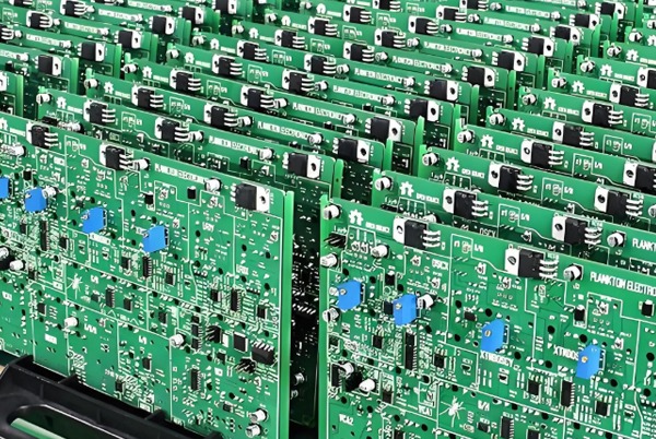
In SMT assembly, terminals – as the core interconnect components – must be collaboratively optimized with other electronic components (such as resistors, capacitors, inductors, and ICs) to ensure circuit performance, reliability, and manufacturability.
1. SMD Resistors and Terminals
Key Considerations:
- Current Path Optimization: High-current resistors (e.g., power resistors) require low-impedance terminal connections to prevent localized overheating.
- Thermal Management: Terminals near high-power resistors should have a good heat dissipation design (e.g., wide copper connections or thermal vias).
- Precision Resistor Matching: High-precision resistors (e.g., 0.1% tolerance) require terminals with low thermal EMF materials (e.g., gold or palladium-nickel plating) to minimize temperature drift effects.
Optimization Solutions:
✔ High-Current Applications: Use high-current-capacity terminals (e.g., copper alloy with thick plating) and optimize PCB copper thickness (≥2oz).
✔ High-Precision Circuits: Use low-contact-resistance terminals (e.g., gold finger contacts) to avoid tin whisker risks.
2. SMD Capacitors and Terminals
Key Considerations:
- High-Frequency Decoupling: Decoupling capacitors (e.g., 0.1μF MLCCs) should be placed as close as possible to IC power pins and connected via low-inductance terminals.
- Bulk Filtering: Terminals for electrolytic capacitors (e.g., 100μF solid capacitors) must support high surge currents to prevent solder joint cracking.
- ESR/ESL Impact: Terminal parasitic resistance/inductance affects the capacitor’s high-frequency performance; optimize layout (e.g., shorten traces).
Optimization Solutions:
✔ High-Speed PCB Design: Use low-ESL terminals (e.g., short-pin or embedded terminals) to reduce loop inductance.
✔ High-Reliability Applications: Choose mechanically shock-resistant terminals (e.g., spring contacts) to prevent capacitor vibration detachment.
3. SMD Inductors and Terminals
Key Considerations:
- Power Inductors: Power inductors in DC-DC circuits (e.g., shielded inductors) require low-loss terminals to minimize DCR (DC resistance).
- High-Frequency Inductors: RF circuit inductors (e.g., 0402 package) must minimize parasitic capacitance/inductance introduced by terminals.
- EMI Suppression: Common-mode inductor terminal layouts should be symmetrical to avoid differential-mode noise coupling.
Optimization Solutions:
✔ Switch-Mode Power Supplies (SMPS): Use wide copper connections for power inductors to reduce conduction losses.
✔ High-Frequency Applications: Select terminals with low parasitic parameters (e.g., microstrip or coplanar waveguide designs).
4. ICs and Terminals
Key Considerations:
- High-Pin-Count Devices (BGA/QFN): Require fine-pitch terminals (e.g., 0.4mm pitch BGA), demanding high precision in PCB manufacturing and assembly.
- High-Speed Signals (PCIe/DDR): Terminal impedance must be matched (50Ω/100Ω differential) to minimize reflection and crosstalk.
- CTE Matching: Terminal materials (e.g., copper alloy) for large ICs (e.g., CPUs/FPGAs) should match PCB CTE (coefficient of thermal expansion) to prevent thermal cycling failures.
Optimization Solutions:
✔ High-Speed Design: Use impedance-controlled terminals (e.g., stripline or embedded capacitance designs) to optimize signal integrity (SI).
✔ High-Reliability Packaging: For automotive/aerospace applications, use vibration-resistant terminals (e.g., press-fit or underfill processes).
5. Other Key Components (Crystals, Transformers, etc.)
| Component Type | Terminal Design Considerations |
|---|---|
| Crystal Oscillators | Low-parasitic-capacitance terminals to avoid frequency drift; minimize trace length to reduce EMI. |
| Transformers/Couplers | High-voltage isolation terminals (e.g., creepage distance ≥8mm/kV); high-current terminals require anti-oxidation plating (e.g., silver or gold). |
| Connectors | Match terminal mechanical strength (e.g., board-to-board connectors need an anti-bending design) to ensure mating cycles (≥500). |
Although SMT chip processing terminals are small components, they play a pivotal role in modern electronics manufacturing. From basic electrical connections to complex signal transmission, the design and processing quality of terminals directly affect the performance and reliability of electronic products. As electronic products evolve toward higher density, higher performance, and smaller sizes, the requirements for terminals are also constantly increasing.


Related Posts