Assemblage du PCB (PCBA) est l'étape au cours de laquelle un le PCB nu se transforme en une carte électronique fonctionnelleLa fabrication de PCB se concentre sur l'étape de fabrication de la carte nue, qui constitue la base du flux de travail complet de fabrication de PCB. Elle comprend le placement des composants, le soudage et les essais rigoureux
La qualité de l'assemblage a une incidence directe :
- Fonctionnalité électrique
- Fiabilité du produit
- Rendement de fabrication
Au TOPFAST, l'assemblage est traité comme un processus axé sur le rendementIl s'agit de veiller à ce que les conseils d'administration soient fonctionnels et solides.
Pour en savoir plus sur les liens entre l'assemblage de circuits imprimés et la fabrication, voir : Fabrication de circuits imprimés et assemblage de circuits imprimés
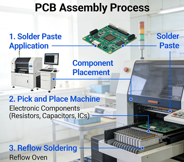
Table des matières
Technologie de montage en surface (SMT) Assemblage
Qu'est-ce que l'assemblage SMT ?
L'assemblage SMT implique le montage composants montés en surface directement sur les pastilles du circuit imprimé à l'aide de :
- Pâte à braser
- Machines Pick-and-Place
- Soudure par refusion
SMT est rapide, précis et adapté aux panneaux à haute densitéLes appareils de la gamme IoT, couramment utilisés dans l'électronique grand public, les télécommunications et les appareils de l'IoT.
Défis SMT
- Les composants à pas fin nécessitent une extrême précision de placement
- Le stress thermique pendant la refusion peut endommager les circuits imprimés si les couches internes ou le placage de cuivre ne sont pas uniformes.
- Les cartes à haute densité augmentent la sensibilité au rendement
Chez TOPFAST, l'assemblage SMT est soigneusement coordonné avec les données de fabrication pour minimiser les défauts et améliorer le rendement.
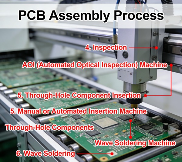
Assemblage des trous de passage
Qu'est-ce que l'assemblage par trous traversants ?
L'assemblage à travers les trous insère les composants avec les fils dans les trous percés et soudés à l'aide :
- Brasage à la vague (brasage en masse)
- Brasage manuel (pour les prototypes ou les cartes de faible volume)
Le trou traversant est encore largement utilisé pour :
- Résistance mécanique
- Composants de haute puissance
- Connecteurs et grands emballages
Flux de travail pour l'assemblage de trous traversants
- Remplissage de trous / Insertion de composants - Insérer les fils des composants dans les trous plaqués
- Soudure - La soudure à la vague ou sélective sécurise les composants
- L'inspection - Contrôles visuels ou AOI de la qualité de la soudure
La qualité du perçage et du placage est directement influencée par Perçage de circuits imprimés et perçage au laseret Explication du processus de cuivrage.
Défis liés aux trous de passage
- Les trous mal alignés ou mal plaqués réduisent la fiabilité du joint de soudure
- L'assemblage manuel augmente le coût de la main-d'œuvre et le risque d'erreur humaine
- Nécessite plus d'espace sur la carte que le SMT
TOPFAST combine perçage et placage de précision avec optimisation de l'assemblage pour maximiser le rendement des trous de passage.
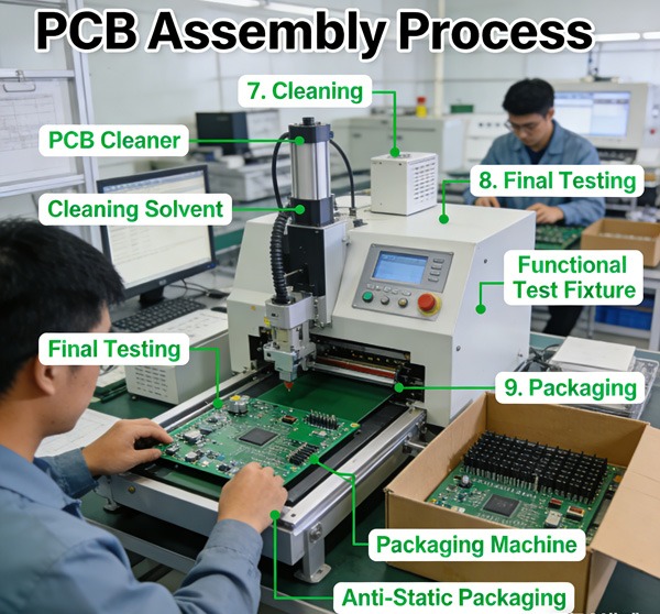
Essais et contrôle de la qualité dans l'assemblage
Test en circuit (ICT)
Contrôles TIC
- Short
- Ouvertures
- Valeurs correctes des composants
Tests fonctionnels
Les tests fonctionnels simulent le fonctionnement réel afin de vérifier que la carte fonctionne comme prévu.
Le test est le dernier point de contrôle qui permet de s'assurer que les étapes de fabrication et d'assemblage sont conformes aux spécifications. Voir aussi Explication du processus de gravure et du contrôle du rendement sur la façon dont la qualité des premières étapes influe sur les résultats des essais.
Considérations sur le rendement de l'assemblage
Rendement
- Qualité de la fabrication (par exemple, couches internes, perçage, placage)
- Précision du placement des composants
- Paramètres de soudure
- Conception de la carte (thermique, espacement, taille des pastilles)
L'assemblage à haut rendement permet de réduire les coûts :
- Remaniement
- Ferraille
- Coût global de production
- Se référer à Fabrication de circuits imprimés et assemblage de circuits imprimés pour comprendre comment les considérations relatives au rendement s'appliquent aux deux processus.
Facteurs de coût dans l'assemblage
Principaux facteurs de coûts :
- Type de composant et emballage
- Densité de la carte et nombre de couches
- Volume d'assemblage (prototype ou production de masse)
- Exigences en matière d'essais et d'inspections
Optimiser l'assemblage sans sacrifier la qualité nécessite alignement étroit entre les processus de conception, de fabrication et d'assemblage.
Conclusion
L'assemblage de circuits imprimés permet de transformer une carte nue en un produit électronique entièrement fonctionnel.
Procédés SMT et de trous borgnesLa fiabilité du produit final est déterminée par des tests rigoureux.
L'intégration avec la qualité de fabrication est essentielle pour y parvenir :
- Rendement élevé
- Une production rentable
- Fiabilité à long terme
FAQ sur le processus d'assemblage des PCB
R : L'assemblage de circuits imprimés consiste à monter des composants électroniques sur un circuit imprimé fabriqué à l'aide de techniques SMT ou de trous traversants, puis à les inspecter et à les tester.
R : La technique SMT consiste à monter les composants sur la surface du circuit imprimé, tandis que la technique du trou traversant consiste à insérer les fils des composants dans les trous percés et à les souder.
R : Des couches mal alignées, des trous mal percés ou un placage incohérent peuvent provoquer des défauts de soudure et réduire le rendement de l'assemblage.
R : L'inspection optique automatisée (AOI), l'inspection par rayons X, le test en circuit (ICT) et le test fonctionnel sont couramment utilisés.
A : TOPFAST aligne les processus de fabrication et d'assemblage, applique des inspections automatisées et manuelles et utilise l'optimisation axée sur le rendement pour une production fiable.