Description
Table of Contents
As a leading one-stop solution provider for communication PCB assembly, we specialize in comprehensive manufacturing services from design to production. Our communication PCB assembly products are widely used in 4G/5G communication equipment, network switches, routers, and various smart communication modules, serving as core components in modern telecommunications infrastructure.
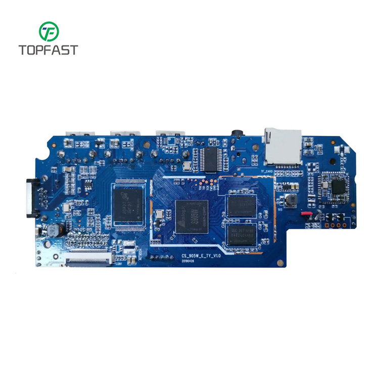
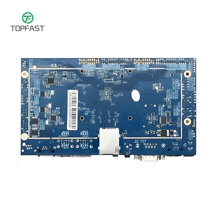
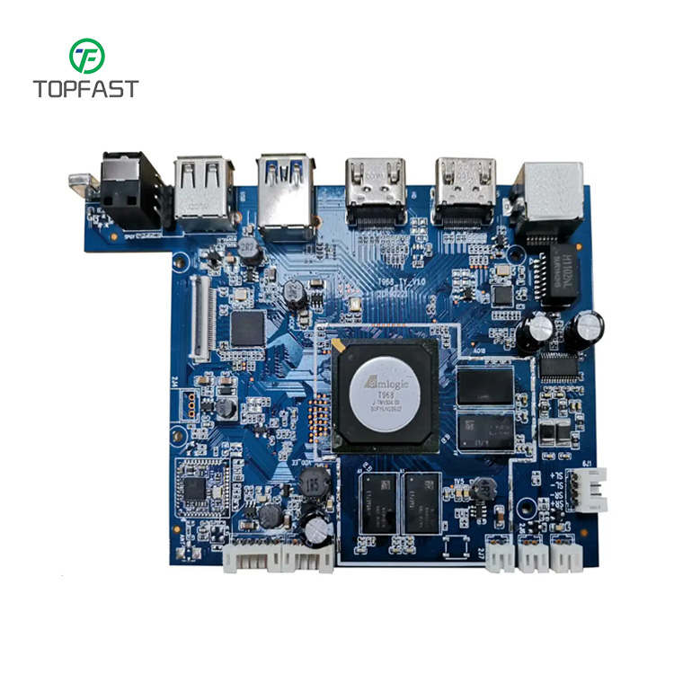
Overview of Communication PCB Assembly Products
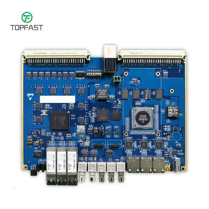
Our 16-layer communication PCB assemblies are manufactured using high-quality FR-4 materials and advanced processes, delivering excellent high-frequency performance and signal integrity to meet the stringent requirements of high-end applications such as AI Android modules. Each product undergoes 100% electronic testing to ensure the highest reliability standards before delivery.
Core Advantages of Our Communication PCB Assembly
Professional Technical Team & Advanced Manufacturing Capabilities
We have an experienced team of communication PCB design engineers and modern production lines capable of handling various communication PCB assembly needs—from simple single-layer boards to complex multilayer designs. Our technical strengths include:
High-Frequency Design Expertise: Proficient in microwave band (700MHz–5GHz) circuit design for optimal 5G device performance.
Precision Machining: Minimum aperture of **0.2mm**, trace width/spacing of **4–6 mil**, supporting high-density interconnects.
Multiple Surface Finishes: Options include **HASL (Lead-Free), ENIG (Immersion Gold), OSP, and Immersion Silver**.
Strict Quality Control: Full-process quality monitoring from raw materials to finished products.
Comprehensive One-Stop Service
We provide a true one-stop solution for communication PCB assembly, covering:
1. Design Support: Schematic design, PCB layout, and signal integrity analysis tailored to customer needs.
2. Flexible Manufacturing: From rapid prototyping to large-scale production.
3. Material Selection: Standard FR-4 to high-frequency materials like Rogers and Taconic.
4. Full Assembly Services: SMT, THT, and full-system testing.
5. Global Logistics: Secure packaging and worldwide shipping for on-time delivery.

Key Technical Features of Communication PCB Assembly
Superior High-Frequency Performance
Our products utilize specialized designs and materials to ensure outstanding high-frequency characteristics:
Low-loss laminates (e.g., Rogers RO4000 series).
Precise impedance control (±5% tolerance).
Optimized stack-up design to minimize crosstalk.
Advanced EMI shielding to reduce RF interference.
Reliable Signal Integrity
For high-speed communication applications, we emphasize:
Strict trace length matching(±50ps skew).
Optimized PDN (Power Delivery Network) design.
Differential pair routing techniques.
Comprehensive ground plane strategies.
Robust Thermal Management
For high-power communication devices, our PCB assembly solutions offer:
High thermal conductivity materials.
Optimized component placement for heat dissipation.
Thermal via arrays.
High-temperature-resistant components.
Applications of Communication PCB Assembly
Our products are widely used in various communication devices:
1. Wireless Communication Systems: 5G base stations, small cells, microwave transmission equipment.
2. Network Infrastructure: Core routers, edge switches, ONU/OLT devices.
3. Terminal Devices: Smartphones, CPEs, IoT communication modules.
4. Specialized Communication Equipment: Military radios, aviation communication, maritime systems.
Custom Communication PCB Assembly Services
We understand the unique needs of different communication applications and offer full customization:
Material Selection: Recommend the best substrate based on frequency and environmental conditions.
Layer Customization: Flexible options from **single-layer to 20+ layers**.
Special Processes: Hybrid boards, heavy copper, rigid-flex PCBs.
Certification Support: Assistance with **CE, FCC, and other industry certifications**.
Quality Assurance & After-Sales Support
We guarantee the highest quality communication PCB assemblies:
100% electrical testing coverage.
Compliance with IPC-A-600 Class 3 standards.
Comprehensive reliability testing (thermal cycling, vibration tests).
Dedicated technical support for design consultation and failure analysis.
Rapid response to customer needs with continuous process improvements.
Why Choose Our Communication PCB Assembly Solutions?
As a professional communication PCB assembly provider, our key differentiators include:
1. Industry Experience: 10+ years specializing in communication PCBs.
2. Technical Leadership: Continuous R&D in high-frequency, high-speed PCBs.
3. Flexible Service Model: Smooth transition from prototypes to mass production.
4. Competitive Pricing: Optimized supply chain for cost efficiency.
5. Reliable Delivery: 95 %+ on-time delivery rate.
Whether you’re developing next-gen 5G devices or upgrading existing communication products, our communication PCB assembly solutions provide expert support. Contact us for more product details and technical consultation.