6-layer PCB Stacking Design and Manufacturing
Electronic products are evolving rapidly, and printed circuit boards (PCBs) have evolved from simple single-layer or double-layer structures to complex multilayer boards with six or more layers to meet the growing demands for component density and high-speed interconnections.
Six-layer PCBs offer engineers greater routing flexibility, improved layer separation capabilities, and optimized cross-layer circuit partitioning solutions. A well-designed six-layer PCB stackup configuration, thickness calculation, manufacturing process, and signal integrity are critical steps in enhancing product performance and reliability.
Table of Contents
6-layer PCB stack configuration
The six conductive copper layers in a multilayer PCB must be arranged in a carefully designed sequence and separated by dielectric materials. A reasonable stacking design is the foundation for ensuring signal integrity, power integrity, and electromagnetic compatibility.
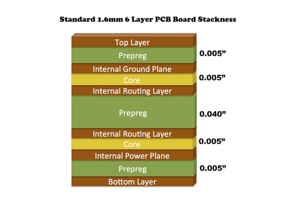
Standard Layer Sequence and Functional Allocation
A typical 6-layer PCB stackup adopts the following layer structure:
- Layer 1 (Top Layer): Component mounting layer for primary devices and partial routing
- Layer 2: Reference plane (typically ground layer GND)
- Layer 3: Inner signal routing layer
- Layer 4: Inner signal routing layer or power plane
- Layer 5: Reference plane (power or ground layer)
- Layer 6 (Bottom Layer): Component mounting and routing layer
This layered structure fully utilizes the advantages of 6-layer boards, providing complete reference planes and optimized return paths for high-speed signals.
Comparison of Three Main Stackup Solutions
Depending on application requirements, 6-layer PCBs primarily feature three stackup approaches:
Solution 1: Symmetrical Layout (Signal Layer Priority)
Layer 1: Signal (Top)
Layer 2: Ground
Layer 3: Signal
Layer 4: Power
Layer 5: Signal
Layer 6: Ground (Bottom)Characteristics:
- Identical reference plane structure above and below the middle layers
- Excellent signal integrity performance
- Widely used in digital, analog, and RF mixed designs
- High routing density suitable for complex designs
Solution 2: Asymmetric Layout (Power-Optimized)
Layer 1: Signal (Top)
Layer 2: Ground
Layer 3: Signal
Layer 4: Power
Layer 5: Power
Layer 6: Ground (Bottom)Characteristics:
- Allows splitting the power plane into multiple regions
- A discontinuous ground plane may affect signal quality
- Suitable for designs requiring complex power distribution
- Relatively lower cost but slightly inferior EMC performance
Solution 3: Hybrid Layout (Signal Integrity Priority)
Layer 1: Signal (Top)
Layer 2: Ground
Layer 3: Signal
Layer 4: Ground
Layer 5: Power
Layer 6: Ground (Bottom)Characteristics:
- Each signal layer has an adjacent reference plane
- Tight coupling between power and ground layers
- Optimal high-speed signal transmission environment
- Sacrifices some routing layers for better SI performance
Golden Rules of Stackup Design
- Signal Layer Adjacency to Reference Planes: Ensure each signal layer has at least one adjacent complete reference plane (GND or Power) to provide low-impedance return paths for high-speed signals.
- Power-Ground Plane Pairing Principle: Arrange power and ground layers on adjacent layers (typically 0.1-0.2mm spacing) to form natural decoupling capacitance and reduce power noise.
- Symmetrical Design: Maintain stackup symmetry where possible to prevent board warping from mismatched thermal expansion coefficients.
- Critical Signal Layer Protection: Route most sensitive high-speed signals on inner layers (Layers 3/4), utilizing outer planes for natural shielding.
Pro Tip: For GHz-level high-speed designs, Solution 3 stackup is recommended. While it sacrifices one routing layer, it delivers optimal signal integrity and EMC performance.
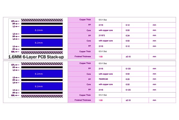
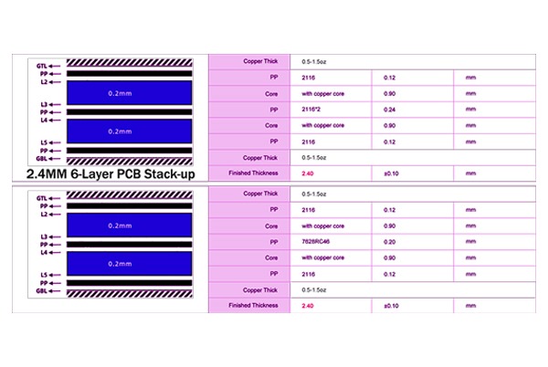
6-Layer PCB Thickness Calculation and Material Selection
PCB total thickness is a parameter that needs to be determined early in design, directly affecting connector selection, mechanical strength, and final product thickness.
Thickness Composition Factors
Three primary factors determine the 6-layer PCB total thickness:
- Copper Layer Thickness:
- Outer layer foil: Typically 1oz (35μm), 0.5oz for high-frequency applications
- Inner layer foil: 1oz or 0.5oz (18μm)
- Plane layers: Recommended 2oz (70μm) for higher current capacity
- Dielectric Layer Thickness:
- Typical values: 8-14mil (200-350μm)/layer
- Materials: FR4, high-speed materials (e.g., Rogers, Isola)
- Thinner dielectrics help reduce interlayer crosstalk
- Lamination Process:
- 2 pressing cycles: First, press the bottom 3 layers, then the top 3 layers
- 3 pressing cycles: Press 2 layers each time for more precise thickness control at a higher cost
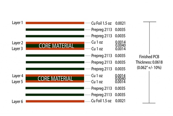
Typical 6-Layer Board Thickness Example
Below is a thickness breakdown for a symmetrically designed 6-layer PCB:
| Layer Type | Thickness | Material Description |
|---|---|---|
| Layer1 (Top) | 35μm | 1oz copper foil |
| Dielectric1 | 254μm | FR4, 10mil |
| Layer2 (GND) | 70μm | 2oz copper foil |
| Dielectric2 | 254μm | FR4, 10mil |
| Layer3 (Signal) | 35μm | 1oz copper foil |
| Dielectric3 | 508μm | Core board, 20mil |
| Layer4 (Signal) | 35μm | 1oz copper foil |
| Dielectric4 | 254μm | FR4, 10mil |
| Layer5 (PWR) | 70μm | 2oz copper foil |
| Dielectric5 | 254μm | FR4, 10mil |
| Layer6 (Bottom) | 35μm | 1oz copper foil |
| Total Thickness | 1.57mm | ~62mil |
Dielectric Material Selection Guide
Common dielectric materials for 6-layer PCBs include:
- Standard FR4:
- Best cost-performance ratio
- Tg value 130-140℃
- Suitable for most consumer products
- High-Speed FR4 (e.g., Isola FR408, Panasonic Megtron6):
- More stable Dk/Df values
- Suitable for GHz-level signals
- 30-50% higher cost than standard FR4
- Specialty Materials (e.g., Rogers RO4350B):
- Ultra-low loss
- For millimeter-wave applications
- 5-10x cost of FR4
Material Selection Considerations:
- Signal frequency: >5GHz recommends high-speed materials
- Budget: High-speed materials significantly increase BOM cost
- Thermal performance: High Tg materials suit high-temperature environments
- Processing difficulty: Some high-frequency materials require special processes
6-Layer PCB Manufacturing Process Flow
6-layer PCB manufacturing is a precise and complex process involving multiple critical steps:
1. Design and Engineering Preparation
- Complete schematic design and layout routing
- Determine layer stackup structure and material specifications
- Perform design rule checks (DRC) and signal integrity analysis
- Generate Gerber, drill, and netlist files
Key Point: Communicate stackup solution with manufacturer early to ensure design aligns with factory capabilities.
2. Inner Layer Pattern Transfer
- Copper Clad Laminate Cleaning: Remove surface oxides and contaminants
- Dry Film Lamination: Apply photosensitive dry film on the copper surface
- Exposure: Transfer circuit pattern to dry film using laser or photoplotter
- Development: Dissolve unexposed dry film areas
- Etching: Remove unprotected copper
- Stripping: Remove remaining dry film to form inner layer circuits
3. Lamination Process
- Layer Alignment: Align layers in sequence with prepreg in between
- Pre-lamination: Initial bonding at low temperature and pressure
- Hot Pressing: Complete curing at high temperature (180-200℃) and pressure
- Cooling and Shaping: Control cooling rate to prevent warping
4. Drilling and Hole Metallization
- Mechanical Drilling: Drill through-holes using carbide drill bits
- Desmearing: Remove resin residue from hole walls
- Electroless Copper Deposition: Deposit a 0.3-0.5μm copper layer on the hole walls
- Electroplating: Thicken the hole copper to 25-30μm
5. Outer Layer Pattern Transfer
Process similar to inner layers, but noting:
- The outer layer foil is thicker (typically 1oz)
- Higher requirements for line width/space control
- Must consider solder mask opening and surface finish
6. Surface Finish and Final Processing
- Solder Mask Application: Protect non-solder areas
- Surface Finish: Options include HASL, ENIG, OSP, etc.
- Silkscreen Printing: Add component designators and markings
- Contour Machining: Mill board edges, V-cut scoring
- Electrical Testing: Open/short testing and impedance testing
Signal Integrity Optimization Techniques
The core challenge in 6-layer PCB design lies in ensuring high-speed signal integrity. Below are key optimization strategies:
1. Impedance Control Design
- Use field solver tools (e.g., Polar SI9000) to accurately calculate:
- Microstrip (outer layer) impedance
- Stripline (inner layer) impedance
- Differential pair impedance
- Typical impedance values:
- Single-ended: 50Ω
- Differential: 100Ω (USB, PCIe, etc.)
Design Essentials:
- Maintain consistent trace width
- Avoid right-angle turns (use 45° or curves)
- Match differential pair lengths (±5mil tolerance)
2. Power Integrity Optimization
- Low-Impedance PDN Design:
- Use thin dielectrics (3-4mil) to enhance power-ground plane coupling
- Properly place decoupling capacitors (combination of large and small values)
- Plane Segmentation Techniques:
- Avoid signal traces crossing split areas
- Ensure sufficient decoupling for each power domain
- Use “island” segmentation for sensitive analog power
3. EMC Design Strategies
- Interlayer Shielding:
- Route high-speed signals on inner layers (Layers 3/4)
- Utilize outer ground planes for shielding
- Edge Treatment:
- Place ground vias every λ/20 spacing
- Keep sensitive signals away from board edges (>3mm)
- Zoning Layout:
- Strictly separate digital/analog areas
- Isolate high-frequency circuits
6-Layer PCB vs 4-Layer PCB: How to Choose?
When to Choose a 4-Layer PCB:
- Medium-low complexity designs
- Smaller board size (<150cm²)
- Signal rates <1Gbps
- Cost-sensitive projects
- Only 2-3 main power domains
When to Upgrade to 6-Layer PCB:
- High-density interconnection needs (e.g., BGA components)
- Multiple power systems (>3 voltage domains)
- High-speed signals (>2Gbps)
- Mixed-signal designs (analog+digital+RF)
- Stringent EMC requirements
- Better thermal management needs
Cost Comparison: 6-layer boards typically cost 30-50% more than 4-layer boards, but an optimized stackup design can reduce board size to partially offset the cost increase.
Professional Design Recommendations and FAQ
Design Checklist
- Is stackup symmetry reasonable?
- Does each signal layer have an adjacent reference plane?
- Is the power-ground plane spacing sufficiently small?
- Do critical signals avoid crossing split areas?
- Does impedance calculation match the manufacturer’s process?
- Have manufacturing tolerances (±10%) been considered?
Frequently Asked Questions
Q1: How to choose dielectric materials for 6-layer boards?
A1: Consider these factors:
- Signal frequency: High frequency requires low Df materials
- Thermal performance: High Tg materials for high-temperature environments
- Budget: High-speed materials significantly increase cost
- Processing difficulty: Some materials require special processes
Q2: How to determine dielectric layer thickness?
A2: Base decision on:
- Target impedance requirements
- Interlayer voltage withstand needs
- Manufacturer process capabilities
- Total thickness limitations
- Signal isolation requirements
Q3: What are the most common mistakes in 6-layer board design?
A3: Most common mistakes include:
- Discontinuous reference planes
- High-speed signals crossing split areas
- Excessive power-ground plane spacing
- Neglecting return path design
- Inaccurate impedance calculations
Professional PCB Manufacturing Service Recommendation
For 6-layer and higher PCBs, choosing an experienced manufacturer is crucial. We recommend considering services with:
✅ Professional multilayer board capability (up to 30 layers)
✅ ±7% impedance control accuracy
✅ Multiple surface finish options (ENIG, OSP, Immersion Silver, etc.)
✅ Free DFM check and engineering support
✅ Quick-turn prototyping (as fast as 48 hours)
Get Instant 6-Layer PCB Manufacturing Quote: Submit Your Requirements
6-layer PCB design is a complex engineering task that requires comprehensive consideration of signal integrity, power integrity, EMC performance, and manufacturing costs. By adopting a reasonable stacking scheme (such as the recommended scheme 3), precise impedance control, and optimized routing strategies, the performance advantages of 6-layer boards can be fully realized.


Related Posts