High Density Interconnector PCB
Table of Contents
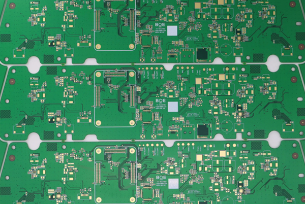
What is HDI?
HDI, which refers to a higher wiring density per unit area than conventional printed circuit boards, is an advanced printed circuit board (PCB) technology that achieves higher levels of electronic component integration through microfine wiring, microscopic via structures, and dense wiring. These boards utilize finer wires and gaps (≤ 100 µm/0.10 mm), smaller vias (<150 µm) and pads (<400 µm/0.40 mm), and higher pad densities (>20 pads/cm2) than conventional PCB technology.
Core Features
- Finer line width/spacing: typically ≤100 µm (0.10 mm), much lower than conventional PCBs (typically 150 µm+).
- Tiny via holes:
- Laser blind-embedded vias: <150 µm in diameter, laser drilled for high-density connections between layers.
- Stacked/staggered holes: Improve vertical space utilization and reduce layer requirements.
- High pad density: >20 pads/cm² to support multi-pin chips (e.g. BGA, CSP packages).
- Thin materials: Use of low dielectric constant, high stability substrates (e.g. FR4, polyimide).
Core features of HDI boards (vs. conventional PCB)
1. Microvia design (laser drilling dominated)
- Technology Choice: HDI boards commonly use laser drilling (hole diameters typically ≤150µm) rather than mechanical drilling. Reasons include:
- Mechanical Drilling Limits: 0.15mm drilling needles are easy to break, have high RPM requirements and low efficiency, and inability to realize the depth control of blind buried holes.
- Laser Advantage: Can process tiny holes (e.g., 50µm), supports Any-layer HDI, and has no physical contact and high yield.
2. Microvia and Hole Ring Designs Via Diameter ≤150µm
- Vias ≤150µm and vias (pads) ≤250µm, freeing up layout space by narrowing the via.
- Example: If the aperture diameter is reduced from 0.30mm to 0.10mm (laser vias), the pad diameter can be reduced from 0.60mm to 0.35mm, saving 67% area.
- Direct Pad Punching (Via-in-Pad): further optimizes BGA/SMD component layout and increases density.
3. High Solder Joint Density (>130 joints/in²)
- Solder pad density determines component integration. HDI realizes multi-functional module high-density assembly (e.g., cell phone motherboards) through micro-miniature holes/wires.
4. High wiring density (>117 wires/in²)
- In order to match the increase of components, the line density needs to be increased simultaneously. HDI achieves complex wiring through fine wiring (line width/spacing ≤100µm) and multilayer stacking.
5. Fine line (line width/space ≤ 3 mil/75µm)
- Theoretical standard: 75µm/75µm, but commonly used in practice, 100µm/100µm. Reason:
- Process cost: 75µm process is demanding on equipment/materials, low yield, few vendors, and high cost.
- Price/Performance Balance: The 100µm solution strikes a balance between density and cost and is suitable for most consumer electronics needs.
Core Benefits of HDI
| Dimension | HDI Board | Traditional PCB |
|---|---|---|
| Drilling Technology | Laser Drilling (Blind Buried Holes, Arbitrary Layers) | Mechanical Drilling (Through Hole Based) |
| Hole Diameter/Hole Ring | ≤150µm/≤250µm | ≥200µm/≥400µm |
| Wiring Density | >117 wires/in² | <50 wires/in² |
| Wire Width/Pitch | ≤100µm (Mainstream) | ≥150µm |
HDI promotes miniaturization and high performance of electronic products through microvia, fine line, and high-density interconnects, and is a key technology for 5G, AI, and portable devices.
HDI PCB Technical Specification Sheet
| Feature | HDI PCB Technical Specifications |
|---|---|
| Layers | Standard: 4–22 layers Advanced: Up to 30 layers |
| Key Highlights | – Higher pad density – Finer trace/space (≤75µm) – Microvias (blind/buried, any-layer interconnect) – Via-in-Pad design |
| HDI Build-Up | 1+N+1, 2+N+2, 3+N+3, 4+N+4, Any-layer (ELIC), Ultra HDI (R&D) |
| Materials | FR4 (Standard/High-performance), Halogen-free FR4, Rogers (for high-frequency applications) |
| Copper Weight (Finished) | 18μm – 70μm |
| Min. Trace/Space | 0.075mm / 0.075mm (75µm/75µm) |
| PCB Thickness | 0.40mm – 3.20mm |
| Max. Board Size | 610mm × 450mm (limited by laser drilling capability) |
| Surface Finish | OSP, ENIG, Immersion Tin, Immersion Silver, Electrolytic Gold, Gold Fingers |
| Min. Hole Size | Mechanical Drilling: 0.15mm Laser Drilling: – Standard: 0.10mm (100µm) – Advanced: 0.075mm (75µm) |
Applications and Core Advantages of HDI Boards
I. Key Application Areas of HDI Boards
With the advancement of semiconductor technology toward miniaturization and high performance, HDI technology has become a critical enabler for modern electronics, particularly dominating the following fields:
- Mobile Communications
- Smartphones (4G/5G): High-density routing supports multi-camera modules, 5G antennas, and high-speed processors (e.g., BGA-packaged chips).
- Base Station Equipment: High-frequency signal transmission (e.g., millimeter-wave bands) relies on HDI’s low-loss materials (e.g., Rogers).
- Consumer Electronics
- Portable Devices: Ultra-thin designs (e.g., foldable smartphone motherboards, TWS earbuds) require HDI’s thin-layer stacking (1+N+1 structure).
- Digital Cameras/AR/VR: High-resolution sensors and miniaturized modules depend on microvias (<75µm) and Via-in-Pad technology.
- Automotive Electronics
- Advanced Driver Assistance Systems (ADAS): Radar and infotainment systems demand HDI’s high reliability (heat resistance, vibration resistance).
- High-Performance Computing
- AI Servers/GPUs: High conductivity and thermal design support high-current transmission (copper thickness ≥70µm).
II. The “Four Highs and One Low” Advantages of HDI Technology
| Advantage | Technical Implementation | Application Value |
|---|---|---|
| High-Density Routing | Trace/space ≤75µm, microvias (laser drilling) | Reduces PCB area by >30%, shrinking end-product size |
| High-Frequency & High-Speed | Low-Dk materials (e.g., PTFE), impedance control (±5%) | Supports 5G/6G mmWave and high-speed SerDes signal integrity |
| High Conductivity | Any-layer interconnect (ELIC), via-filling plating technology | Reduces interlayer signal delay, improves data rates |
| High Insulation Reliability | Halogen-free substrates, precision lamination (≤3% expansion rate) | Meets automotive AEC-Q200 certification, extends lifespan by 50% |
| Low Cost | Fewer layers (e.g., replacing 8-layer through-hole PCBs with 4-layer HDI), automated laser drilling (yield >98%) | Reduces total cost by 15%-20% |
III. Market Outlook and Supporting Data
- Growth Trend: From 2000–2008, global HDI board production grew at a CAGR of >14% (Prismark data). By 2023, the market size exceeded $12 billion, with a projected 2030 CAGR of 8.3%.
- Technology Evolution: Ultra HDI (trace/space ≤40µm) and embedded component technology will further drive AIoT and wearable device development.
With its “Four Highs and One Low” characteristics, HDI technology serves as a core driver of electronics industry advancement, holding immense potential in 6G communications, autonomous vehicles, and quantum computing.
Classification of HDI Boards
HDI boards are categorized into three main types based on the stacking method and lamination count of blind vias:
(1) 1+N+1 Type
- Structure: Features a single lamination layer for high-density interconnects.
- Characteristics:
- Most cost-effective HDI solution
- Suitable for designs with moderate complexity
- Typical applications: Entry-level smartphones, consumer electronics
(2) i+N+i (i≥2) Type
- Structure: Incorporates two or more lamination layers for high-density interconnects.
- Key Features:
- Supports staggered or stacked microvia configurations
- Advanced designs often use copper-filled stacked microvias
- Provides enhanced routing density and signal integrity
- Applications:
- Mid-to-high range mobile devices
- Networking equipment
- Automotive electronics
(3) Any-Layer Interconnect (ELIC) Type
- Structure: All layers utilize high-density interconnects with stacked copper-filled microvias.
- Advantages:
- Enables complete design freedom for interlayer connections
- Optimal solution for ultra-high pin count components (e.g., CPUs, GPUs)
- Maximizes space utilization in compact designs
- Typical Use Cases:
- Flagship smartphones
- High-performance computing
- Advanced wearable devices
Technical Comparison
| Type | Lamination Count | Via Structure | Cost Factor | Typical Applications |
|---|---|---|---|---|
| 1+N+1 | Single lamination | Basic microvias | Lowest | Entry-level consumer electronics |
| i+N+i (i≥2) | Multiple laminations | Stacked/staggered microvias | Moderate | Mid-range mobile/networking |
| ELIC | All-layer | Copper-filled stacked vias | Highest | High-end computing/mobile |
This classification system helps designers select the appropriate HDI technology based on performance requirements, complexity, and cost considerations. The evolution from 1+N+1 to ELIC represents increasing capabilities to support more advanced electronic applications.
HDI/BUM PCB Material Performance Requirements
The development of materials for HDI printed circuit boards has always focused on meeting the “four highs and one low” requirements (high density, high frequency, high conductivity, high reliability and low cost). The increasing miniaturization and performance needs of printed circuit boards are being met by improving properties such as resistance to electromigration and dimensional stability.
1. Prepreg (PP) Materials
- Composition: Resin + reinforced materials (typically fiberglass)
- Advantages:
- Low cost
- Good mechanical rigidity
- Wide applicability
- Limitations:
- Moderate reliability (weaker CAF resistance)
- Lower pad peel strength (not suitable for drop-test demanding applications)
- Typical Applications: Mid-to-low end consumer electronics (e.g., budget smartphones)
2. Resin Coated Copper (RCC) Materials
- Types:
- Metallized PI film
- PI film + copper foil laminated with adhesive (“Pure PI”)
- Cast PI film (liquid PI cured on copper foil)
- Advantages:
- Excellent manufacturability
- High reliability
- Superior pad peel strength (ideal for drop-test applications)
- Enabled microvia laser drilling technology
- Limitations:
- Higher cost
- Lower overall rigidity (potential warping issues)
- Impact: Pioneered the transition from SMT to CSP packaging
3. Laser Drillable Prepreg (LDP) Materials
- Positioning: Cost-performance balance between PP and RCC
- Advantages:
- Better CAF resistance than PP
- Improved dielectric layer uniformity
- Meets/exceeds international standards for pad peel strength
- Applications: Mid-to-high end mobile devices and electronics
4. Liquid Crystal Polymer (LCP) Materials
- Key Properties:
- Ultra-low dielectric constant (Dk=2.8 @1GHz)
- Minimal loss tangent (0.0025)
- Inherent flame retardancy (halogen-free)
- Superior dimensional stability
- Advantages:
- Ideal for high-frequency/high-speed designs
- Environmentally friendly
- Challenging traditional PI dominance
- Applications: High-end RF/microwave circuits, advanced packaging
Material Selection Guide
| Material | Cost | Reliability | High-Freq | Rigidity | Best For |
|---|---|---|---|---|---|
| PP | Low | Moderate | No | High | Budget consumer devices |
| RCC | High | Excellent | Moderate | Low | Drop-test sensitive apps |
| LDP | Medium | Good | Limited | High | Premium mobile devices |
| LCP | Very High | Exceptional | Yes | Medium | 5G/RF/advanced packaging |
Difference in PCB manufacturing process between core-containing boards and coreless boards
I. Core-Based HDI Manufacturing Process
1. Core Board Characteristics
- Structural Design:
- Uses through-holes or hybrid buried/blind/through-hole structures (typically 4-6 layers)
- Optional metal-core construction (enhanced thermal dissipation)
Technical Parameters:
| Parameter | Core Board | Buildup Layers |
|---|---|---|
| Through-hole diameter | ≥0.2mm | ≤0.15mm (microvias) |
| Trace/space width | ≥0.08mm | ≤0.08mm |
| Interconnect density | Low | Ultra-high density |
2. Core Board Functions
- Mechanical support (ensures rigidity)
- Electrical interconnection bridge between the buildup layers
- Thermal management (especially for metal-core boards)
3. Key Pretreatment Processes
- Via treatment: Via filling + surface planarization
- Surface treatment: Electroless copper plating + electroplating (1-3µm thickness)
- Pattern transfer: LDI laser direct imaging (±5µm precision)
II. Breakthrough Coreless HDI Technology
1. Representative Technologies
- ALIVH (Any Layer Interstitial Via Hole)
- B²IT (Buried Bump Interconnection Technology)
2. Revolutionary Advantages
| Comparison | Core-Based HDI | Coreless HDI |
|---|---|---|
| Structure | Core + buildup zones | Homogeneous layer design |
| Interconnect Density | Significant layer variation | Uniform ultra-high density (+40% vs. core) |
| Signal Transmission | Longer paths (core-induced delay) | Shortest possible paths |
| Thickness Control | Limited by core (≥0.4mm) | Can achieve <0.2mm |
3. Core Process Innovations
- Layer interconnection:
- Replaces electroless copper with conductive paste or copper bumps
- Laser ablation for any-layer microvias (≤50µm diameter)
- Reliability assurance:
- Nanoscale surface roughening (Ra≤0.5µm)
- Low-cure dielectric materials (Tg≥200℃)
Concluding Remarks
Driven by advances in laser drilling, materials science, and multilayer stacking, HDI PCBs represent the cutting edge of miniaturization and high-performance electronics. HDI technology will continue to evolve as devices demand higher speeds, lower latency, and higher reliability, pushing the limits of PCB manufacturing.


Related Posts