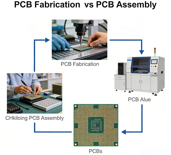
Understanding the difference between PCB fabrication and PCB assembly is essential for engineers, designers, and manufacturers.PCB fabrication and PCB assembly are two core stages of the overall PCB manufacturing process.
- PCB fabrication produces the bare board, including layers, drilling, plating, and etching.
- PCB assembly (PCBA) adds components, soldering, and testing to create a functional electronic board.
A holistic view of both processes is critical for:
- Optimizing design for manufacturability
- Controlling cost and yield
- Ensuring reliable final products
This hub page links to detailed sub-articles explaining each step and strategy, reflecting the professional practices used by TOPFAST, a PCB manufacturer focused on process reliability and yield optimization.
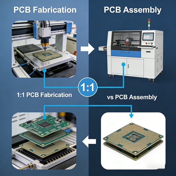
Table of Contents
Understanding PCB Fabrication
PCB fabrication involves the creation of the bare board, which forms the foundation for all subsequent assembly processes.
Key fabrication steps include:
- Inner layer fabrication (read more)
- Drilling vias (read more)
- Copper plating (read more)
- Etching (read more)
- Applying solder mask and silkscreen
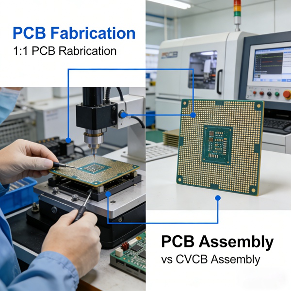
For a detailed explanation of the fabrication process and how it affects assembly and reliability, see: PCB Fabrication vs PCB Assembly: Key Differences.
Why it matters: Fabrication quality determines mechanical strength, electrical integrity, and first-pass yield, directly impacting assembly efficiency.
Understanding PCB Assembly
PCB assembly is the step where a bare board becomes a functional PCB by adding and soldering electronic components.
Assembly includes:
- Surface Mount Technology (SMT) (read more)
- Through-Hole Assembly (read more)
- Inspection and Testing (read more)
- PCB Assembly Process Explained: SMT, Through-Hole, and Testing
- Cost & Yield Optimization in Fabrication vs Assembly
Why it matters: Even perfectly fabricated boards can fail if assembly is not carefully controlled. Component placement, soldering, and testing define product reliability.
Key Differences Between Fabrication and Assembly
| Aspect | Fabrication | Assembly |
|---|---|---|
| Focus | Bare board creation | Component mounting and soldering |
| Core Processes | Layer stacking, drilling, plating, etching | SMT, through-hole, soldering, testing |
| Main Challenges | Yield, copper quality, drill accuracy | Component placement, solder quality, and inspection |
| Cost Drivers | Layer count, copper weight, tolerances | Component type, placement complexity, testing |
For a step-by-step breakdown of each process, visit PCB Fabrication vs PCB Assembly: Key Differences.
Cost and Yield Optimization Across Processes
Optimizing cost and yield requires considering both fabrication and assembly simultaneously:
- Reduce fabrication costs by optimizing layer count, copper distribution, and panel utilization.
- Reduce assembly costs by streamlining component placement, soldering efficiency, and inspection processes.
- Early design review (DFM) ensures compatibility with both processes and maximizes yield.
TOPFAST Approach: Professional Manufacturer Perspective
At TOPFAST, the approach to PCB fabrication and assembly emphasizes:
- Process integration: Fabrication and assembly are treated as an end-to-end system.
- Yield-driven manufacturing: Continuous monitoring and DFM feedback reduce defects.
- Reliability and repeatability: Ensuring high-quality boards with consistent performance.
This perspective ensures that cost, yield, and quality are optimized simultaneously, not in isolation.
Conclusion
PCB fabrication and assembly are interdependent processes.
- Fabrication quality sets the foundation for reliable assembly.
- Assembly practices define the final product’s functionality and reliability.
- Cost and yield optimization requires collaboration between design, fabrication, and assembly teams.
This hub, along with its linked sub-articles, provides a comprehensive understanding of PCB manufacturing and assembly workflows, reflecting professional practices from TOPFAST without marketing bias.
PCB fabrication and assembly FAQ
A: Fabrication creates the bare board, while assembly adds components and performs soldering and testing.
A: Poor fabrication (misaligned layers, insufficient plating, or drilling defects) can lead to assembly errors and lower yield.
A: Optimize layer count, copper distribution, panelization, component placement, soldering processes, and inspection.
A: Surface Mount Technology (SMT) and through-hole assembly, followed by inspection and testing, are standard.
A: TOPFAST integrates fabrication and assembly into a yield-driven, process-monitored workflow to ensure high-quality, cost-effective PCBs.