Prototype PCB Assembly
Table of Contents
What is prototype PCB assembly?
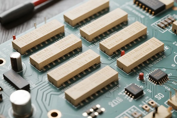
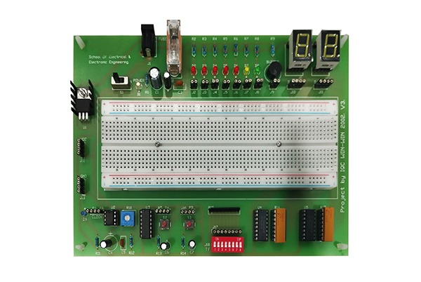
A PCB prototype is an example of a product designed to demonstrate whether an idea for a design can be successfully implemented. Most prototypes only focus on how easy they are to use, but PCB prototypes must also be practical so that the circuit design can be fully tested. When the PCB prototype is being put together, engineers can try out different ways to design and make it. They determine the best way to design and set up the product by testing and comparing various options. This ensures that the product does what it’s supposed to and can be relied on.
Advantages of Prototype PCB Assembly
1. Shortened Timeline and Cost Savings
Making a prototype PCB (printed circuit board) lets you test out different designs and manufacture it quickly and cheaply. Specific benefits include:
1) Comprehensive Testing
Prototype PCBs allow engineers to quickly and accurately identify design flaws. If we don’t have samples to check, finding problems will take much longer. This could mean late deliveries, unhappy customers, and money lost.
2) Improved Client Communication
Clients often want to see the product at various stages of development. If you give us a model of what you want, it helps us to understand what you want clearly. This means there will be fewer misunderstandings and less time spent on communication and redesign requests.
3) Reduced Rework
Testing with a model PCB lets engineers check how well the board works before making it in large quantities, so they don’t have to spend money on making changes later on. Defects found after production has started require more time and resources to resolve.
2. Smother Manufacturing and Production Process
Using a professional prototype PCB assembly service makes it easier to communicate and helps avoid common errors, including:
| Issue Type | Description | Value of Prototype Services |
|---|---|---|
| Version Confusion | Multiple design versions accumulate due to client or team changes, making it hard to identify the best one. | Helps track and confirm the optimal version through clear communication. |
| Design Blind Spots | Limited experience in certain PCB types may lead to subtle issues. | Multidisciplinary expertise identifies and addresses potential flaws. |
| DRC Limitations | DRC tools may not optimize trace geometry, size, or length. | Professional insight supplements automated checks to improve design quality |
Experienced prototype suppliers can spot these problems early on and suggest ways to improve the prototype before it is made. This makes sure the prototype is better for testing and for making in the future.
3. Early Testing and Functional Validation
Using accurate and reliable PCB prototypes makes it easier to solve design problems during the development process. High-quality models show how the final product will perform, and let engineers check:
1) PCB Design
Early detection of design flaws through prototyping helps minimize project cost and time.
2) Functional Testing
Theoretical designs may not always work in practice. Prototypes allow comparison between expected and actual performance.
3) Environmental Testing
Products are often used in specific situations, such as when the temperature changes, the power supply is unstable, or there is a physical impact.. Prototypes undergo simulated environmental tests to ensure reliability.
4) Final Product Design
Prototypes help us work out if we need to change the PCB layout, materials, or product packaging.
4. Isolated Component Testing
Prototype PCBs are highly useful for testing individual components and specific functions:
1) Design Theory Validation
Simple prototypes allow engineers to verify design concepts before moving further into the development process.
2) Decomposing Complex Designs
Breaking down a complex PCB into basic parts that all do one thing helps make sure each part works correctly before they are all put together. This makes it easier to spot and fix problems.
5. Cost Reduction
It’s important to make a model of the product so that you can see if it will work before making a lot of the product. This is because making a lot of the product is expensive. It also helps you to see if the product will work and deal with any problems.
1 Early Defect Detection
The earlier a flaw is found, the cheaper it is to fix. Prototypes prevent problems from reaching mass production, protecting the budget.
2) Product Adjustment Identification
Changes in PCB shape or materials can affect overall product specifications. Prototypes help work out early on if changes are needed, which reduces the cost of redesigning the product and its packaging later on.
In short, using a prototype PCB assembly helps make better products that work well and are reliable. It also makes them cheaper and means they can be sold more quickly.
PCB Prototyping Specifications
1. Dimensions
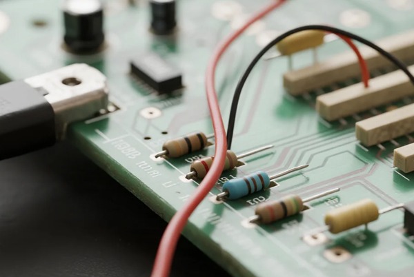
PCB cost is proportional to its surface area. Reasonable-sized planning helps control costs. Irregular shapes can lead to material waste, while smaller rectangular boards are generally more cost-effective.
Case: The initial version of a relay shield board had an area of 74.5 cm² with unused space. The optimized prototype version was reduced to 65.4 cm², significantly saving costs.
2. Layer Count
The number of layers is a key indicator of PCB complexity. Each additional copper layer acts like an “elevated highway,” enabling more complex electrical interconnections within limited space.
3. Material Type
Multilayer PCBs are typically made from stacked copper-clad laminates. The most commonly used material is FR-4 (glass epoxy), known for its flame-retardant properties.
⚠️ Note: High-speed or RF boards require special attention to the dielectric constant and thickness of materials.
4. Board Thickness
Thickness is usually determined by the number of copper layers and the structure. Standard thickness is ≥1.0 mm. If space is limited, it can be reduced to 0.4 mm, but this must be confirmed with the manufacturer.
5. Surface Finish
Surface plating improves solderability and oxidation resistance. Common types include:
| Type | Characteristics | Applications |
|---|---|---|
| HASL (Lead/Lead-Free) | Low cost, moderate flatness | Standard circuit boards |
| ENIG (Electroless Ni/Au) | High cost, high flatness, strong oxidation resistance | BGA components, test points, high-precision applications |
The image on the left shows an ENIG coating, which is flat and uniform; the right shows HASL, with visible unevenness.
(Image comparison can be included here)
6. Impedance Control
High-frequency circuits (e.g., Wi-Fi, Bluetooth) require impedance control to ensure signal integrity. Impedance is influenced by dielectric material, trace width, solder mask, etc.
For example, Wi-Fi antennas often require 50Ω impedance. Higher impedance requirements increase costs.
7. Trace Width/Spacing
Refers to the minimum width of copper traces and the minimum distance between traces. Finer widths and spacing demand higher manufacturing precision. Designs must align with process capabilities to avoid yield reduction.
8. Hole Size
The size of vias and drill holes directly affects manufacturing difficulty. Smaller holes save space but require stricter tolerances and may increase scrap rates.
9. Solder Mask
The solder mask prevents soldering shorts. Common colors include green, red, blue, black, and white.
For example, white solder mask is prone to discoloration during high-temperature reflow (left), while black (right) avoids such cosmetic defects.
(Image comparison can be included here)
10. Silkscreen
Used for labeling component designators, graphics, and logos. LPI (Liquid Photo Imaging) offers higher resolution than traditional silkscreen, making it suitable for high-precision needs, though at a slightly higher cost.
The image below compares LPI (left) and traditional silkscreen (right) at the same magnification.
(Image comparison can be included here)
11. Pin Pitch
Refers to the distance between adjacent pins on a component. Fine-pitch components (e.g., QFN, BGA) require high-precision assembly, which may increase costs and scrap rates.
12. Castellated Pads
Suitable for PCB designs requiring interlocking or stacking. Castellated pads enhance mechanical fixation and electrical connection.
The left image shows a PCB with castellated pads; the right shows it assembled onto a mainboard.
(Image comparison can be included here)
13. RoHS Compliance
It is recommended to clearly communicate RoHS (Restriction of Hazardous Substances) compliance requirements to manufacturers to avoid the use of non-compliant materials (e.g., lead-containing substances), which could impact product environmental compliance and market access.
Prototype PCB Assembly Process:
PCB assembly is a critical step in electronic product manufacturing. The SMT assembly manufacturing process directly impacts product performance, production efficiency, and cost control.
Pre-Assembly Preparation
Adequate preparation is essential for ensuring a smooth production process and final product quality.
1. Design File Validation
- PCB Design Review: Carefully examine client-provided design files, including board dimensions, component layout, and pad design compatibility with SMT requirements.
- DFM Analysis: Identify potential manufacturing issues such as insufficient clearance, improperly sized pads, or thermal imbalance.
2. Component Procurement and Inspection
- Supplier Selection: Source components from certified suppliers complying with international standards (e.g., ISO, IPC).
- Incoming Quality Control (IQC): Perform visual inspections, electrical testing, and authenticity verification to eliminate defective components.
✅ Key Note: Only components passing strict inspection can proceed to assembly.
SMT Assembly Process
Surface Mount Technology involves highly precise and automated steps to ensure reliable connections.
1. Solder Paste Printing
Solder paste printing accuracy directly affects soldering quality.
| Factor | Requirement | Impact |
|---|---|---|
| Stencil | High-precision laser-cut | Ensure paste volume and alignment |
| Solder Paste | Optimal viscosity and composition | Prevents defects like bridging or insufficient solder |
| Squeegee | Controlled pressure and speed | Guar uniform deposition |
⚠️ Even minor deviations can cause defects such as bridging, insufficient solder, or misalignment.
2. Component Placement
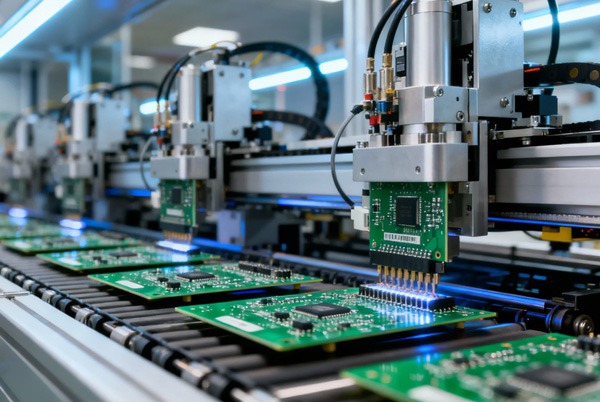
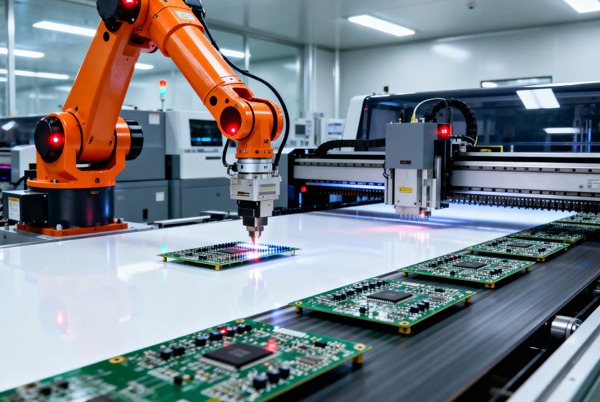
Modern pick-and-place machines ensure high-speed, high-accuracy mounting.
- Vision Systems: Recognize component orientation, polarity, and position.
- Placement Accuracy: Within ±0.05mm for chips and passive components.
- Nozzle and Feeder Setup: Regular maintenance and calibration are necessary to sustain performance.
3. Reflow Soldering
The reflow process melts solder paste to form permanent electrical connections.
- Temperature Profiling: Customized curves based on PCB thickness, component sensitivity, and paste specification.
- Thermal Zones:
- Preheating: gradual temperature ramp to activate flux.
- Soaking: uniform heat distribution.
- Reflow: peak temperature to melt solder.
- Cooling: controlled solidification of joints.
🌡️ Incorrect temperature settings may lead to tombstoning, cold joints, or component damage.
Post-Assembly Quality Testing
Rigorous inspection and testing ensure product functionality and reliability.
1. Visual Inspection
- Automated Optical Inspection (AOI): Scans for missing components, misalignment, bridging, or skewed parts.
- X-ray Inspection: Examines hidden connections such as BGA soldering and internal vias.
2. Functional Testing
- Electrical Tests: Continuity, resistance, voltage, and current checks.
- In-Circuit Test (ICT) / Flying Probe: Validates electrical performance and signal integrity.
- Burn-in Testing: Simulates real-world operating conditions to screen early failures.
Quality Assurance and Continuous Improvement
A systemic approach to quality control ensures consistent and reliable output.
- Full Traceability: Track materials, processes, and test results for each board.
- Statistical Process Control (SPC): Monitor key process parameters to detect deviations early.
- Root Cause Analysis & Corrective Actions: Address recurring issues through process optimization and staff training.
- Feedback Loop: Incorporate lessons learned into future designs and assembly runs.
Precautions for Prototype PCB Assembly
I. Surface Mount Technology (SMT) Assembly
1. Pre-Assembly Preparation
- PCB Cleaning: PCBs must be thoroughly cleaned and dried before assembly to prevent moisture from affecting soldering quality.
- Component Verification: Prepare components according to the BOM list, paying special attention to the orientation and specifications of polarized components.
2. SMT Operation
- Feeding and Setup: Load materials as required by the pick-and-place machine and accurately configure parameters.
- Placement Execution: Ensure proper calibration of placement coordinates and control placement speed and temperature to avoid material throwing or misalignment.
3. Soldering and Inspection
- Soldering Quality Check: Focus on identifying issues such as bridging, tilting, reversal, or tombstoning. Use AOI or microscopy for confirmation.
II. Through-Hole Technology (THT) Assembly
1. Pre-Assembly Preparation
- PCB Cleaning: Ensure the board surface is clean and dry.
- Component Preparation: Verify THT component specifications and installation orientation. Pre-form leads if necessary.
2. Soldering Operation
- Tantalum Capacitor Handling: Clearly distinguish between positive and negative terminals before installation.
- Soldering Control: Manage solder volume and soldering time to ensure full solder joints without short circuits.
3. Post-Soldering Inspection
- Visual and Mechanical Check: Confirm solder joint robustness, correct component alignment, board integrity, and absence of flux residue.
III. Common Issues and Solutions
(1) SMT Assembly Issues
| Issue Type | Possible Causes | Solutions |
|---|---|---|
| Misalignment/Shift | Nozzle clogging, coordinate deviation | Clean nozzle, recalibrate placement coordinates |
| Reversed Placement | Incorrect component orientation | Check polarity markings, ensure proper insertion |
| Contamination/Oxidation | Improper storage or solder paste contamination | Clean with a specialized cleaner (e.g., STD-120) |
(2) THT Soldering Issues
| Issue Type | Possible Causes | Solutions |
|---|---|---|
| Board Burning | Excessive temperature or prolonged heating | Adjust the iron temperature to the appropriate range, and control soldering time |
| Short Circuits | Excessive solder, closely spaced pins | Reduce solder amount, use desoldering braid, maintain pin spacing |
| Solder Balls/Beading | Insufficient preheating, moist solder paste | Increase preheating, store and handle solder paste properly, lightly sand pads if necessary |
💡 Tip: It is recommended to document issues in real time during assembly and provide feedback to the production team to continuously optimize process parameters and improve yield.
Application Fields
Consumer Electronics
Smartphones, laptops, and other consumer electronic devices utilize high-density interconnect (HDI) PCBs to integrate complex components, ensuring high-speed and stable signal transmission and collaboration between high-performance processors, multi-camera modules, and sensors.
Automotive Electronics
- Autonomous Driving Systems: PCBs connect sensors such as cameras, radars, and LiDARs to enable high-speed transmission and real-time processing of environmental data.
- Engine Control Units (ECUs): PCBs precisely control critical parameters like fuel injection and ignition timing, directly impacting vehicle power and emissions performance.
Industrial Control
In industrial automation and smart factories, PCBs provide reliable connections and signal relay for sensors, PLC controllers, and actuators, enabling precise and collaborative control of production processes.
Medical Devices
Medical equipment (e.g., ultrasound devices, patient monitors, and medical imaging systems) relies on high-performance PCBs for signal amplification, filtering, and digital-to-analog conversion, ensuring data accuracy and diagnostic reliability.
Communication Equipment
Devices such as 5G base stations, optical modules, and routers use high-frequency PCBs to optimize radio frequency signal paths, reduce transmission loss, and ensure high-speed and stable communication networks.
Artificial Intelligence
AI training servers and inference devices leverage multi-layer PCBs and substrates to achieve high-speed interconnections between GPUs/ASICs, supporting large-scale model parameter synchronization and efficient computing, thereby facilitating the development of intelligent computing centers.
Premium Supplier
Topfast, founded in 2008, is a one-stop PCB solution provider with 17 years of experience, specializing in rapid prototyping and small-batch production. We offer end-to-end services including PCB design, manufacturing, and assembly.
Our product range covers HDI boards, heavy copper boards, rigid-flex boards, high-frequency and high-speed boards, semiconductor test boards, and more, widely used in industries such as telecommunications, medical devices, industrial controls, automotive electronics, and aerospace. All products comply with IPC standards and are certified with UL, RoHS, and ISO 9001.
Adhering to a customer-first and quality-driven philosophy, we utilize advanced production equipment (including laser drilling machines, AOI inspection systems, VCP production lines, etc.) and a professional technical team to provide high-quality and reliable customized services.
Related Posts