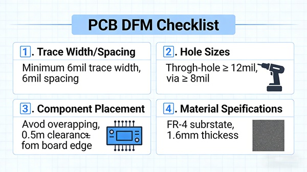
Blog

PCB-Substrat-Material

PCB-Substrat-Material

This article provides an in-depth analysis of key factors in PCB substrate selection, including comparisons of FR-4, polyimide, and high-frequency materials, copper foil selection techniques, and considerations for solder mask and surface finishes. It specifically addresses five common substrate issues engineers face and offers practical solutions to help avoid pitfalls and optimize PCB design and manufacturing processes.

PCB-Oberflächenbehandlungen

Was sind PCB-Oberflächenveredelungen?

From consumer electronics to aerospace equipment, PCB surface finishes critically impact product reliability. This guide examines 7 mainstream processes at the microstructural level, compares costs/performance, reveals failure mechanisms like ENIG black pad and OSP carbonization, and provides optimal selection strategies for different budgets/requirements.

PCB-Layout-Design

PCB-Layout-Design

This comprehensive guide walks through the entire PCB layout workflow—from schematics to final checks—detailing best practices for grid settings, component placement, special part handling, routing approaches, and verification methods. It also provides actionable solutions to five frequent design challenges, offering value to both novices and experienced designers seeking to elevate their PCB quality.

Leiterplatte

Was ist die Funktion von PCB??

This comprehensive guide explores PCB boards from design to application, covering their manufacturing process, six core functions (electrical connection, mechanical support, thermal management, etc.), and solutions to common problems like signal integrity and BGA defects. We delve into material selection, design considerations, and future trends like flexible PCBs and AI-assisted design, providing practical insights for engineers and electronics enthusiasts to optimize PCB performance and reliability.

PCB-Herstellung

Prozessablauf bei der PCB-Herstellung

This comprehensive guide explores the detailed workflow of printed circuit board manufacturing, breaking down each critical step from panel cutting to final testing. It examines basic processes such as inner-layer imaging, lamination, drilling, plating, and surface treatment, while emphasizing key design considerations and quality control measures.

PCB

PCB-Arbeitsprinzip

Erfahren Sie, wie Leiterplatten (PCBs) funktionieren, von der Signalübertragung und Stromverteilung bis hin zu Multilayer-Design und Wärmemanagement.

PCB-Design

Was ist ein PCB-Design?

Beherrschen des Leiterplattendesigns mit Kenntnissen über Komponenten, bewährte Layoutverfahren, Signalintegrität, Wärmemanagement und branchenübliche Testmethoden.

Spannungsregler

Spannungsregler

Discover everything about voltage regulators – from working principles and types (linear, switching, LDO) to applications in automotive, industrial, and renewable energy systems. Learn about key specifications, selection criteria, troubleshooting, and future trends (SiC, GaN, digital control). Perfect for engineers, designers, and tech enthusiasts!”

PCB Pars Check

PCB Pars Check

Umfassender Leitfaden zu PCB-Prüfmethoden und Designinspektionscheckpunkten - von AOI bis zu Funktionstests - zur Sicherung der Leiterplattenqualität. Beherrschen Sie 8 wichtige Prüftechniken und eine vollständige Checkliste für die Entwurfsprüfung, um Produktionsrisiken zu verringern und die Produktzuverlässigkeit zu verbessern.

    • Jetzt zitieren

      Kostenloses Angebot

    • WhatsApp