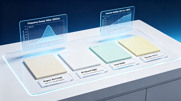
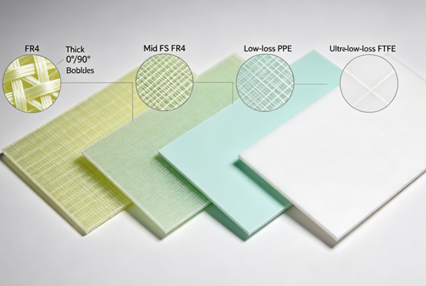
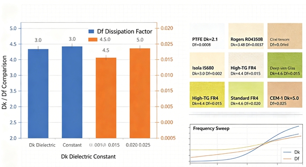
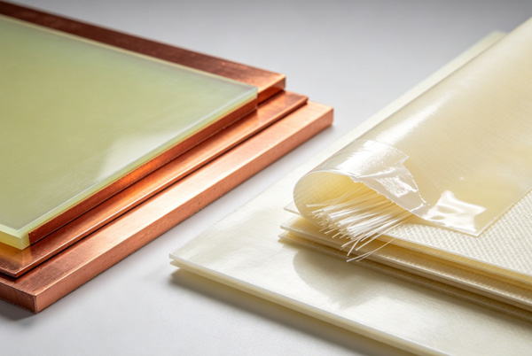
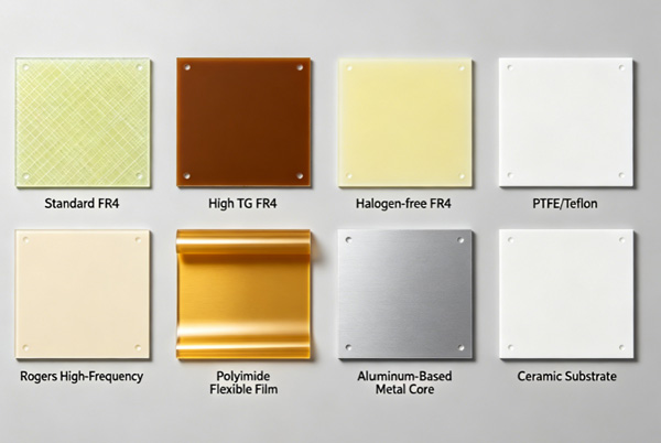
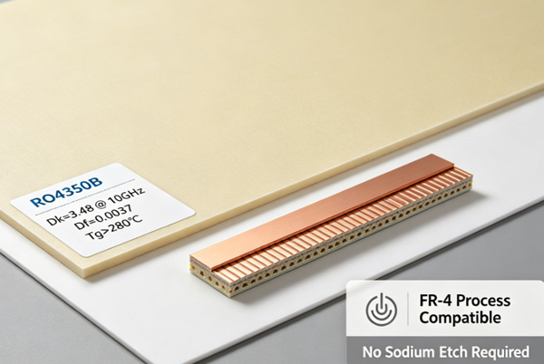
TOPFAST PCB One-Stop Solutions

Blog

PCB copper foil

How Copper Weight Deeply Affects PCB Design

This article analyzes the impact of copper weight on PCB design. It examines how thickness affects electrical performance, heat dissipation, and manufacturing costs. The guide addresses five key areas: high-frequency design, current carrying calculations, heavy copper board challenges, lightweight solutions, and EMC optimization. With practical data and case studies, it provides selection guidelines for different applications (5G RF, automotive, consumer electronics) and a quick-reference table for design decisions.

ICT Test Fixture

ICT Test Fixtures

This guide covers everything about ICT test fixtures for electronics manufacturing. Learn how they work to verify component placement, polarity, and solder quality. We address 5 practical challenges – high costs, test point access, programming complexity, maintenance needs, and detection limits – with actionable solutions. Includes fixture selection guidelines, design tips, and strategies to build a complete quality system. Discover future trends and why ICT remains essential for reliable manufacturing.

In-Depth Analysis of High-Voltage PCB Safety Design

Redefining high-voltage PCB spacing design through multi-physics analysis. This guide integrates materials science (CTI mechanisms), failure physics (CAF models), and environmental dynamics for intelligent spacing solutions. Features advanced insulation design, simulation techniques, and standards compliance for mission-critical applications in power/automotive/medical electronics.

PCB Impedance

Outer Copper Layer Thickness and Trace Impedance Control

This article explains how outer copper thickness impacts trace impedance in high-speed PCB design. It covers impedance principles, copper thickness effects (0.5-2oz), key design rules, and manufacturing factors. Discover TOPFAST’s solutions for signal integrity in 5G/AI applications.

PCB Solder Mask Design

Six Common Solder Mask Mistakes Every PCB Designer Should Know

Solder mask design is crucial for PCB reliability. This article covers 6 common errors: insufficient clearance, opening inaccuracies, misalignment, weak solder dams, silkscreen conflicts, and poor testability design. It explains root causes and provides solutions for both standard and high-frequency/high-voltage designs. Includes actionable checklist for better manufacturability.

1 2 31