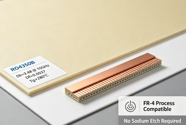
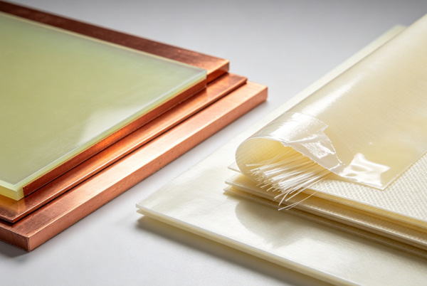
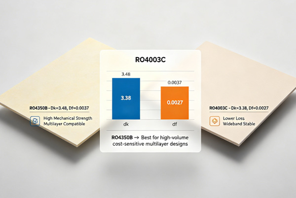
Blog

hdi pcb

What is the lamination structure of HDI PCB boards?

HDI PCBs are a core technology for the miniaturization of modern electronic devices, and their laminate structure design directly determines product performance and reliability. From simple single-layer lamination (1+4+1) to complex double-layer lamination (1+1+4+1+1), key design considerations are provided to achieve the optimal balance between space constraints, signal integrity, and manufacturing costs.

PCB manufacturing equipment

What equipment do professional PCB manufacturers use?

A complete set of equipment covering the entire process from substrate cutting, inner layer circuit production, multilayer board lamination, precision drilling, electroplating, outer layer circuit production, solder mask printing, to final testing. High-tech PCB-specific equipment is the technical foundation for the complexity and precision of circuit board manufacturing.

PCB reflow soldering

How to perform reflow soldering on double-sided PCB?

Double-sided PCB reflow soldering is a core process in electronics manufacturing, involving the selection of solder paste and red glue processes, temperature curve control, and dual-sided soldering strategies. This article analyzes the soldering process for double-sided PCBs, provides solutions to common issues, and offers tips for process optimization to improve soldering yield and production efficiency.

PCB copper thickness

What is the standard thickness of the copper layer on a PCB?

PCB copper foil thickness standards (35μm-210μm), including IPC-2152 current-carrying capacity formulas, signal integrity impact, thermal management solutions, and copper thickness selection strategies for typical applications such as consumer electronics, automotive electronics, and high-power equipment.

PCB shape

How important is shape when manufacturing PCB?

PCB shape design directly affects the mechanical strength, signal integrity, and production cost of circuit boards. Excellent PCB shape design requires balancing functional requirements with process limitations, considering multiple factors such as trace angles, edge treatment, and material selection.

ic

What is the difference between integrated circuits and PCB?

Want to know the difference between integrated circuits and PCBs? Compare the core differences between IC chips and circuit boards in terms of function, structure, manufacturing, and application, and analyze their different roles and synergistic relationships in electronic devices.

pcb

Where can I order inexpensive double-sided PCBs?

The unique advantages of leading domestic PCB procurement platforms (such as Lichuang and Yunhan Xincheng) and Topfast, including free prototyping, tiered pricing, fast delivery times, and full-chain services, help you obtain high-quality PCBs at the lowest cost.

PCB soldering

How to determine if a PCB is soldered correctly?

PCB soldering quality directly affects the performance and reliability of electronic products. Professional testing methods (such as AOI, X-ray, flying probe testing, etc.) help you accurately identify soldering issues and provide solutions to ensure high-quality PCB production.

PCB soldering

Does a development board made of PCB require soldering?

Whether a PCB development board requires soldering depends on its completion level and usage scenario. Finished development boards are typically pre-soldered and ready for immediate use; semi-finished boards may require additional soldering of pin headers or peripherals; blank PCBs require complete soldering.

Welding flaw detection

PCB Welding flaw detection

Welding, as an indispensable joining process in modern industry, directly affects the safety and service life of engineering structures. According to statistics, more than 60% of structural failure accidents are caused by welding defects, making welding flaw detection a key part of quality control.

    • Get a quote

      Get the best discount

    • Online Consultation