Kretskortstillverkning är en flerstegs, noggrant kontrollerad process där små avvikelser kan leda till tillförlitlighetsproblem, produktionsförluster eller ökade kostnader.
Även om många resurser beskriver PCB-tillverkning på en hög nivå, är det viktigt att förstå hur varje tillverkningssteg samverkar med nästa är avgörande för:
- Utformning av tillverkningsbara kort
- Kontroll av kostnader
- Säkerställer långsiktig tillförlitlighet
Denna artikel ger en steg-för-steg-översikt över tillverkningsprocessen för mönsterkortmed länkar till fördjupade förklaringar av varje kritiskt skede.
Perspektivet återspeglar verkliga tillverkningsmetoder som används av professionella PCB-tillverkare, t.ex. TOPFASTdär processtabilitet och avkastningskontroll är centrala prioriteringar.
Innehållsförteckning
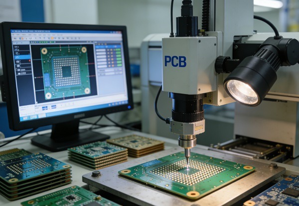
Översikt över Tillverkningsprocess för kretskort
Ett typiskt arbetsflöde för tillverkning av mönsterkort omfattar:
- Tillverkning av inre skikt
- Borrning (mekanisk eller laser)
- Kopparplätering
- Etsning av mönster
- Inspektion och avkastningskontroll
Varje steg bygger vidare på det föregående. Fel som begås tidigt i processen kan ofta inte korrigeras senare.
Tillverkning av inre lager
Tillverkningen av det inre skiktet är grunden för tillverkning av flerlagers mönsterkort.
I det här skedet:
- Kopparfolien är mönstrad för att bilda interna kretsar
- Måttnoggrannhet är avgörande
- Defekterna är permanent låsta i stapeln efter lamineringen
Eftersom innerskikten inte kan repareras när de väl har laminerats tillämpar tillverkarna strikta processkontroller och inspektionsstandarder.
För en detaljerad förklaring av förberedelse av det inre lagret, bildtagning och etsning, se:
Förklaring av innerskiktets tillverkning
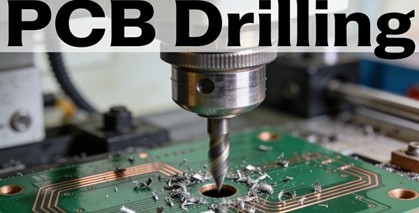
Borrning av kretskort: Skapa anslutningar mellan skikten
Borrning skapar de hål som senare blir vior och genomgående hålanslutningar.
Två primära borrmetoder används:
- Mekanisk borrning
- Laserborrning
Varje metod har avvägningar i:
- Storlek på hål
- Aspect ratio
- Kostnad
- Tillförlitlighet
Felaktig borrning påverkar direkt pläteringskvaliteten och via tillförlitligheten.
För att förstå när mekanisk borrning eller laserborrning är lämpligt, läs:
PCB-borrning kontra laserborrning
Process för kopparplätering
Kopparplätering förvandlar borrade hål till elektriskt ledande vertikala anslutningar.
Pläteringsprocessen omfattar:
- Elektrolös deponering av koppar
- Uppbyggnad av elektrolytisk koppartjocklek
Pläteringens kvalitet avgör:
- Via väggens hållfasthet
- Prestanda vid termisk cykling
- Strömförande förmåga
Inkonsekvent plätering är en vanlig orsak till fel i fält, även när korten klarar de första elektriska testerna.
För en fullständig genomgång av pläteringssteg och tillförlitlighetsfaktorer, se:
Förklaring av kopparpläteringsprocessen vid PCB-tillverkning
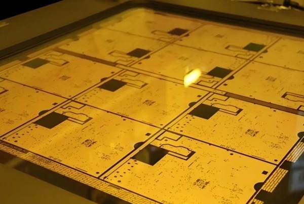
Etsning av kretskort och kretsbildning
Etsning avlägsnar oönskad koppar för att definiera det slutliga kretsmönstret.
Detta steg måste balansera:
- Koppartjocklek
- Noggrannhet i linjebredd
- Kontroll av avstånd
Överetsning eller underetsning leder till:
- Öppnar eller shorts
- Variation i impedans
- Minskat utbyte vid tillverkning
Etsningsprestanda blir alltmer kritiska när konstruktionerna går mot finare spår och högre lagerantal.
För en djupgående titt på etsningskemi och påverkan på utbytet, läs mer:
Förklaring av PCB-etsningsprocessen och Yield Control
Avkastningskontroll genom hela tillverkningsprocessen
Utbytet styrs inte i ett enda steg - det är resultat av kumulativ processtabilitet.
Viktiga drivkrafter för avkastning är bl.a:
- Noggrannhet i inre skikt
- Borrens kvalitet
- Pläteringens enhetlighet
- Etsningskonsistens
Professionella PCB-tillverkare övervakar kontinuerligt utbytesdata för att:
- Identifiera processglidning
- Optimera designreglerna
- Minska skrot och omarbetningar
På TOPFAST integreras feedback om avkastning i DFM-granskningar för att hjälpa kunderna att undvika dolda tillverkningsrisker innan produktionen påbörjas.
För en tillverkningsinriktad översikt över drivkrafter för avkastning, se:
Förklaring av PCB-etsningsprocessen och Yield Control
Hur designbeslut påverkar tillverkningsprocessen
Ur tillverkningssynpunkt har många PCB-problem sitt ursprung i designval som t.ex:
- Alltför fina spårvidder
- Vior med högt aspektförhållande
- Obalanserad distribution av koppar
- Alltför snäva toleranser
Tidigt samarbete mellan konstruktörer och tillverkare hjälper till att anpassa konstruktionen till processens kapacitet.
Detta tillvägagångssätt minskar:
- Iterationer
- Förseningar i produktionen
- Total ägandekostnad
Tillverkarens perspektiv: Processintegration hos TOPFAST
Som en professionell PCB-tillverkare ser TOPFAST PCB-tillverkning som en integrerat systeminte enstaka steg.
Viktiga principer inkluderar:
- Stabila processfönster
- Tidig identifiering av DFM-risker
- Avkastningsdriven optimering
- IPC-anpassade kvalitetsstandarder
I stället för att enbart fokusera på minimispecifikationer ligger tyngdpunkten på repeterbarhet, tillförlitlighet och skalbar produktion.
Slutsats
Tillverkningsprocessen för mönsterkort är en sekvens av steg som är beroende av varandra och där kvaliteten byggs upp successivt och inte kontrolleras i slutet.
Genom att förstå hur tillverkning av innerskikt, borrning, kopparplätering och etsning fungerar tillsammans kan ingenjörer och inköpare:
- Fatta bättre designbeslut
- Minska tillverkningsrisken
- Kontrollera kostnaderna utan att ge avkall på kvaliteten
Denna översikt fungerar som en inkörsport till djupare tekniska förklaringar av varje kritiskt steg och återspeglar verkliga metoder som används av erfarna mönsterkortstillverkare som TOPFAST.