Accurate Calculation of PCBA Costs: A Comprehensive Guide from BOM to Quotation
In the field of electronic product development, accurate PCBA cost estimation is a critical factor for project success. Component costs typically account for 40%-60% of the total PCBA cost, and even a small decimal error can lead to losses in the tens of thousands of dollars. This article provides a complete PCBA cost calculation system to help hardware engineers, procurement specialists, and project managers make smarter decisions.
Table of Contents
1. Complete Picture of PCBA Cost Structure
PCBA cost is a multi-dimensional, comprehensive system, mainly comprising the following six modules:
| Cost Module | Typical Percentage | Key Influencing Factors |
|---|---|---|
| Component Procurement Cost | 40%-60% | Chip type (standard components vs. high-end BGA), supply chain stability, purchase quantity |
| PCB Manufacturing Cost | 10%-20% | Layer count (4-layer board is ~2x cost of 2-layer), board material type, size, process complexity |
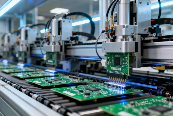
| SMT Assembly Cost | 5%-15% | Number of SMT placement points, component type, batch size |
| Testing & Quality Control Cost | 3%-8% | Number of test points, reliability requirements (can reach >10% for medical/automotive) |
| DIP Through-Hole Assembly Cost | 2%-5% | Number of through-hole components, soldering method (wave soldering vs. manual) |
| Auxiliary Materials & Overhead Cost | 2%-7% | Solder paste, stencil, equipment depreciation, etc., unit cost decreases with larger volumes |
💡 Key Insight: Component cost has the highest proportion, especially noticeable in projects reliant on high-end chips. Rational control of component procurement is the core of cost optimization.
2. PCB Cost Calculation and Design Optimization Strategies
2.1 PCB Cost Calculation Formula
PCB Cost = Laminate Material Cost + Process Cost + Special Treatment Fees
- Laminate Material Cost Calculation:
Single PCB laminate cost = Price per square meter of PCB ÷ Number of PCBs producible per square meter - Process Cost Factors:
- Drilling cost: Number of holes × Aperture coefficient (more holes, smaller aperture = higher cost)
- Trace width/clearance: Precision traces <0.2mm/0.2mm increase cost by 30%-50%
- Layer count cost: Each additional layer increases cost by 40%-60%
- Surface finish: ENIG (Immersion Gold) is 20%-30% more expensive than HASL (Lead-free)
- Special Process Surcharges:
- Impedance control: Increases cost by 10%-15%
- Blind/Buried vias: Increase cost by 25%-40%
2.2 PCB Design Optimization Strategies
- Panel Utilization Optimization: Rational panelization design can increase utilization from 70% to over 85%, potentially reducing cost by 10%-15%.
- Process Simplification Principles:
- Avoid unnecessarily small via diameters (<0.3mm)
- Keep trace width/clearance ≥0.15mm
- Reduce special via plating requirements
3. BOM Management Standardization Process
Efficient BOM management is the foundation of cost control:
- Export BOM list from schematic
- Consolidate identical component models
- Standardize naming conventions (e.g., use uF/nF consistently for capacitor values)
- Annotate key parameters: Tolerance, voltage rating, package size
- Distinguish between alternate and sole-source part numbers
Example BOM before optimization:
C1: 0.1uF, C2: 100nF, C3: 104 → After standardization: All unified to "0.1uF"
4. Detailed SMT Assembly Cost Calculation
4.1 SMT Placement Point Calculation Rules
| Component Type | Point Calculation Standard |
|---|---|
| Standard SMD (Resistor/Capacitor/Diode) | 2 points per component |
| Small Chip (e.g., SOT-23) | 3 points per component |
| Medium Chips (QFP/QFN, etc.) | Based on actual pin count |
| Large Chips (BGA/LGA, etc.) | Based on actual pin count |
SMT Cost = (SMT Placement Points × Unit Price) + Stencil Fee + Setup Charge
4.2 Surface Finish Process Cost Comparison
| Process Type | Relative Cost (HASL as Baseline) | Applicable Scenarios |
|---|---|---|
| HASL (Lead-free) | 1.0 (Baseline) | Cost-sensitive products |
| Lead-free HASL | 1.2-1.3 | Products requiring RoHS compliance |
| OSP | 1.0-1.2 | Simple consumer electronics |
| ENIG | 2.0-2.5 | High-reliability products |
5. DIP Through-Hole and Testing Cost Calculation
5.1 DIP Through-Hole Cost Calculation
DIP Cost = (DIP solder joint count × Unit Price) + Wave Solder Fixture Cost
- Manual soldering unit price: ¥0.08-0.15 per solder joint
- Wave soldering unit price: ¥0.03-0.08 per solder joint
- Fixture cost: ¥500-3000 (reusable)
5.2 Testing Cost Composition
Testing Cost = (Flying Probe Test Points × Unit Price) + Functional Test Development Fee + Test Fixture Cost
6. Total PCBA Cost Calculation Formula and Practical Application
6.1 Complete Cost Calculation Formula
Total PCBA Cost = PCB Cost + [Component Cost × (1 + Loss Factor)] + SMT Cost + DIP Cost + Testing Cost + Packaging & Logistics Cost + (Profit & Management Fee)
6.2 Quick Reference Formulas (Estimation Baseline)
- Standard 2-layer board (1.6mm FR4) + standard components ≈ ¥8-15 per 100 points
- 4-layer board + precision components ≈ ¥15-28 per 100 points
7. Five Major Strategies for PCBA Cost Optimization
7.1 DFM (Design for Manufacturing) Optimization
- Set reasonable trace width/clearance (≥0.15mm)
- Avoid excessively small via diameters that increase production difficulty
7.2 Component Procurement Strategy
- Consolidated Purchasing: Combine demands to obtain quantity discounts.
- Domestic Alternatives: Use domestic components where performance requirements are met.
7.3 Production Batch Optimization
- Consolidate small batch orders to reduce line changeover frequency.
- Plan lead times rationally to avoid rush charges (can increase cost by 15%-25%).
7.4 Process Route Selection
- Simple boards: Lead-free solder paste process.
- Boards with large components: Red glue + wave soldering solution.
- High-density boards: Solder paste printing + reflow soldering.
7.5 Testing Scheme Optimization
- Prototype/Small batch: Flying probe test.
- Mass production: Dedicated test fixture (can reduce cost by 60% post-volume production).
8. PCBA Quotation Process and Time Management
A typical complete PCBA quotation cycle is as follows:
Material Confirmation (1-3 days) → PCB Quotation (1 day) → Component Quotation (1-4 days) → Assembly Fee Quotation (1-2 days)Tips to Shorten Quotation Cycle:
- Provide a complete BOM list, Gerber files, and process requirements.
- Mark long-lead-time components (e.g., FPGAs, specific processors) in advance.
- Establish long-term cooperative relationships with suppliers.
Conclusion
PCBA cost estimation is a systematic project that requires comprehensive consideration of multiple links, such as design, materials, process, and testing. By understanding the cost structure, mastering calculation methods, and implementing optimization strategies, companies can not only accurately control costs but also enhance market competitiveness while ensuring quality.
Cost control is not simply about bargaining down prices, but a value creation process achieved through design optimization, process innovation, and supply chain collaboration.

Related Posts