Cracked vias and barrel cracks are among the most critical latent reliability failures in PCB manufacturing.
These defects often pass initial electrical testing but fail later under thermal or mechanical stress, making them especially dangerous in high-reliability applications.
This article explains:
- What are via cracks and barrel cracks are
- Why they occur
- How they are detected
- How manufacturers reduce their occurrence
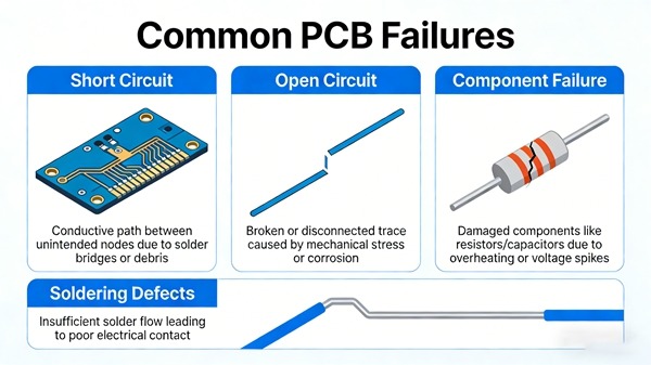
Table of Contents
What Are Via Cracks and Barrel Cracks?
Via Crack
A via crack is a fracture in the copper plating of a via, typically at:
- The knee of the via
- The interface between copper and dielectric
Barrel Crack
A barrel crack refers specifically to a circumferential crack in the plated via barrel.
Both interrupt electrical continuity over time.
Why Via Cracks Are a Serious Reliability Issue
Via cracks are dangerous because they:
- Are often intermittent
- Worsens with thermal cycling
- Are difficult to detect visually
They frequently appear only after field use or stress testing.
Failure overview:
Common PCB Failures Explained
Primary Causes of Via and Barrel Cracks
Z-Axis Expansion Mismatch
During heating, dielectric materials expand more than copper in the Z-axis.
Repeated expansion and contraction create stress in the via barrel.
Thin or Non-Uniform Copper Plating
Insufficient plating thickness reduces the via’s ability to absorb mechanical stress.
Process detail:
Copper Plating Process in PCB Manufacturing
High Aspect Ratio Vias
High aspect ratio vias are more challenging to plate uniformly and experience greater stress.
Excessive Thermal Cycling
Repeated exposure to:
- Reflow soldering
- Power cycling
- Environmental temperature changes
Accelerates crack formation.
Reliability testing:
PCB Thermal Reliability Testing
Design Factors That Increase Via Crack Risk
Certain design decisions significantly increase risk.
High-Risk Design Choices
- Very small via diameters
- Thin PCB thickness with deep vias
- Large copper planes without relief
- Dense via-in-pad structures
Design-for-reliability review is critical.
Manufacturing Factors Contributing to Via Cracks
Drilling Quality
Drill smear, rough hole walls, or fiber pull-out weaken copper adhesion.
Comparison:
PCB Drilling vs Laser Drilling
Inadequate Desmear Process
Poor desmear prevents proper copper bonding to the dielectric.
Plating Stress Control
Improper plating chemistry can introduce internal stress into copper deposits.
How Via Cracks Are Detected
Via cracks are rarely detected by surface inspection alone.
Common Detection Methods
- Thermal stress testing
- Micro-section analysis
- Electrical testing after cycling
- X-ray inspection (limited effectiveness)
Inspection overview:
PCB Inspection & Testing Explained
Preventing Cracked Vias and Barrel Cracks
Design-Level Prevention
- Adequate via diameter
- Controlled aspect ratio
- Thermal relief patterns
Process-Level Prevention
- Optimized drilling parameters
- Uniform copper plating thickness
- Stress-controlled plating chemistry
Material Selection
- Low Z-axis expansion materials
- High-Tg laminates for thermal stability
Manufacturers like TOPFAST integrate via reliability considerations early in process planning.
Relationship to Other PCB Failure Modes
Via cracks often coexist with:
- Delamination
- CAF formation
- Intermittent open circuits
Related topic:
PCB Delamination Causes and Prevention
Conclusion
Cracked vias and barrel cracks are not random defects but predictable outcomes of thermal stress, design decisions, and process limitations.
Through:
- Proper design practices
- Controlled manufacturing processes
- Appropriate material selection
Their occurrence can be significantly reduced.
Via Cracks in PCB FAQ
A: No. Once cracked, vias cannot be reliably repaired.
A: No. Many are latent and intermittent.
A: Not always, but sufficient and uniform thickness is critical.
A: Yes, due to higher reflow temperatures.
A: Usually not unless cracks are severe.