In the field of PCB design, copper foil weight (typically measured in ounces per square foot, oz) is not only a fundamental parameter but also a critical variable affecting the overall performance, reliability, and cost of the circuit board. As electronic products evolve toward higher frequencies, higher power, and greater integration, the proper selection of copper foil weight has become a core competency that engineers must master. As a professional PCB manufacturer, TOPFAST will comprehensively explore the multifaceted impact of copper foil weight across dimensions, including electrical performance, thermal management, mechanical strength, manufacturing costs, and lightweighting trends. We will also provide selection strategies tailored to diverse application scenarios.
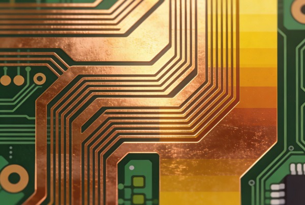
Table of Contents
Electrical Performance: Balancing Current Carrying Capacity, Impedance, and High-Frequency Response
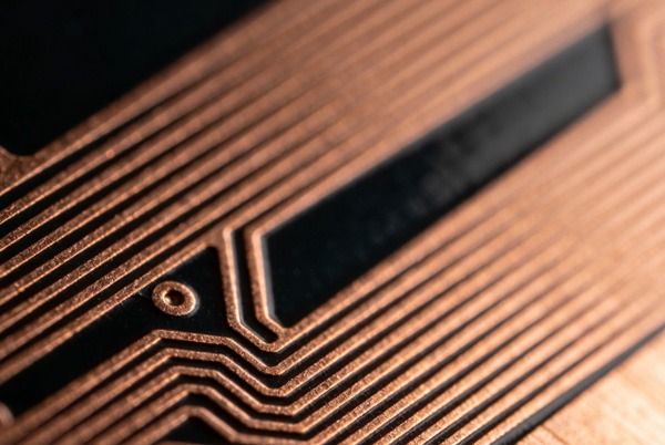
1. Current Carrying Capacity and DC Resistance
Copper thickness directly affects the conductor’s cross-sectional area, thereby determining its current-carrying capacity and resistance. According to IPC-2152 standards, under the same temperature rise conditions, 2 oz copper can carry approximately 60%–80% more current than 1 oz copper. For example, 1 oz copper (≈35 µm thick) can carry about 1.5 A per 1 mm trace width, while 2 oz copper (≈70 µm) can exceed 2.5 A. For high-current paths (e.g., power modules, motor drivers), increasing copper thickness is a direct way to reduce voltage drop and power loss.
2. Signal Integrity and High-Frequency Response
In high-frequency applications (e.g., 5G RF, DDR5 memory), signal transmission exhibits a significant “skin effect” where current concentrates on the conductor’s surface. In such cases, the surface roughness of the copper foil has a greater impact on insertion loss than its thickness. Low-roughness materials, such as very low profile (VLP) or reverse-treated foil (RTF), can deliver superior signal integrity at high frequencies, even at thicknesses as low as 0.5 oz (≈18 µm). For millimetre-wave bands, precise etching control is necessary to maintain impedance, and excessively thick copper can increase process difficulty and lead to impedance deviation.
Thermal Management: The Critical Role of Copper as a “Heat Spreader”
1. Optimising Heat Conduction Paths
Copper boasts a thermal conductivity as high as 400 W/(m·K). Thick copper foil rapidly dissipates heat from localised sources—such as power MOSFETs and processors—through lateral diffusion, preventing hotspot formation. Field testing shows that PCBs with 2 oz copper foil achieve surface temperatures 12–15°C lower than 1 oz versions under identical power dissipation. In high-temperature environments like automotive electronics and industrial power supplies, thick copper layers often serve as “thermal bridges” to direct heat toward heat sinks or dedicated heat dissipation components.
2. Stack-up Design and Thermal Coupling
In high-density multilayer boards, vertical thermal conduction pathways can be established by placing thick copper inner layers (e.g., 2–3 oz) beneath critical heat-generating components and pairing them with thermally conductive vias. This “thermal via + thick copper plane” combination is commonly employed in thermal management designs for high-performance chips such as FPGAs and ASICs.
Mechanical and Reliability: From Vibration Tolerance to Solder Joint Lifespan
1. Structural Reinforcement and Vibration Tolerance
In vibrating environments such as automotive, aerospace, and industrial controls, thick copper foil enhances the overall mechanical strength of the PCB. Copper thicknesses of 3 oz or more can increase the board’s flexural strength by over 150% while also improving the copper plating integrity of plated through-holes, reducing the risk of cracks due to mechanical stress.
2. Soldering and Long-Term Reliability
Appropriately increasing the copper thickness in the pad area (such as by incorporating localised copper blocks) can improve thermal capacitance balance and reduce defects like cold solder joints and incomplete soldering. During thermal cycling tests, thick copper designs mitigate stress caused by CTE mismatch, enhancing product longevity in temperature-varying environments.
Cost and Manufacturing: The Trade-off Between Feasibility and Economics
1. Non-linear Increase in Material Cost
The relationship between copper weight and cost is not linear. For instance, the material cost of 3 oz copper foil is approximately 110% higher than that of 1 oz. As thickness increases, hidden costs such as etching chemical consumption, drill bit wear, and yield control also rise significantly.
2. Process Challenges and Design Compromises
Thick copper foil (≥3 oz) imposes stricter requirements on the etching process: increased side etching effects necessitate wider minimum line widths/spacing; poor copper flow during lamination often leads to insufficient fill or resin voids. Consequently, thick copper designs frequently require relaxed design rules or hybrid processes such as stepped copper or localised thickening.
Lightweight Trends: Rebalancing Performance with Thinner Copper Foil
In fields like consumer electronics, aerospace, and portable devices, weight is a critical metric. Copper foil accounts for 15%–30% of a PCB’s total weight, making thickness reduction a key approach to lightweighting:
- Ultra-Thin Copper Foil Applications: Copper foils as thin as 9 µm (≈0.25 oz) and 12 µm (≈0.3 oz) are widely used in HDI boards, flexible circuits, and chip substrates, achieving minimal weight while maintaining sufficient current-carrying capacity.
- Localised Optimisation Strategies: Using thick copper (e.g., 2 oz) only in power paths and ground planes, while employing 1 oz or thinner copper for signal layers, can reduce overall weight by over 30%.
- Material Innovations: New materials like composite copper foils (e.g., copper-graphene) and surface-treated foils (low roughness) offer improved electrical and thermal performance at the same thickness, providing new avenues for lightweight design.
Application Scenario Selection Matrix: From Consumer Electronics to Industrial Power
| Application Scenario | Recommended Copper Weight | Key Considerations | Typical Examples |
|---|---|---|---|
| High-Frequency RF/Millimetre Wave | 0.5 oz (≈18 µm) | Surface Roughness, Impedance Control | 5G Antennas, Radar RF Front-Ends |
| Consumer Electronics Motherboards | 1 oz (≈35 µm) | Cost, Lightweight, General Current Carrying | Smartphones, Laptops |
| Automotive BMS/Motor Drivers | 2 oz (≈70 µm) | High Current Carrying, Vibration Tolerance | Battery Management, Motor Control Units |
| Industrial Power Supplies/Inverters | 3–4 oz (≈105–140 µm) | Extreme Current, Thermal Requirements | Server Power Supplies, PV Inverters |
| High-Density Interconnect (HDI) | 0.5–1 oz (≈18–35 µm) | Fine Trace Width, Microvia Processing | Wearables, High-End Motherboards |
| Flexible Circuits (FPC) | 0.3–0.5 oz (≈9–18 µm) | Flexibility, Weight | Foldable Screen Hinges, Sensors |
Design Recommendations: A Systematic Trade-off Methodology
- Current-First Principle: Determine minimum copper thickness based on path current, with a 30% margin according to IPC-2152 curves.
- High-Frequency Precision Control: Prioritise low-roughness thin copper for signals >1 GHz, and use field solvers to verify impedance and loss.
- Electro-Thermal Co-Simulation: Utilise simulation tools (e.g., ANSYS Icepak, Cadence Celsius) to analyse electrical and thermal performance simultaneously, avoiding local overheating.
- Cost Sensitivity Analysis: During prototyping, evaluate the BOM cost and yield impact of different copper weight options to find the optimal cost-performance point.
Conclusion
The selection of copper foil weight is fundamentally a multi-objective optimisation balancing electrical performance, thermal management, mechanical reliability, and cost. As technologies like AIoT, electric vehicles, and high-frequency communications evolve, copper foil materials and processes continue to innovate. Looking ahead, application-driven “intelligent copper thickness allocation” and the adoption of copper-nonmetallic composite materials may usher in breakthroughs for PCB design. Engineers must transcend single-parameter thinking and embrace system-level co-design to achieve the optimal balance between performance, reliability, and cost-effectiveness.
Five Core Issues in PCB Copper Foil Weight
A: Key Point: For signals >1GHz, prioritise copper foil surface roughness over thickness.
Recommendation: 0.5oz Very Low Profile (HVLP/RTF) copper, with impedance deviation controllable within ±3%.
Note: For millimetre-wave bands (e.g., 77GHz), pair with surface roughness ≤5µm.
A: Standard: Follow IPC-2152, considering multilayer board heat dissipation and ambient temperature.
Common Mistake: Avoid simple rules like “1oz = 1.5A/mm”; inner layer traces require 30% derating.
Case Study: Measured current capacity in electric vehicle power modules is 25-30% lower than theoretical values.
A: Etching: Process time increases by 150%, trace width should be ≥8mil.
Yield: Typically 30% lower than standard boards.
Cost: Processing costs increase by 80-120%.
A: Strategy: Local heavy copper (2oz in power areas / 1oz in signal areas) + grid copper pour.
New Materials: Copper-graphene composite foil can reduce weight by 30%.
Effect: Drone PCB weight reduced by 18% after thinning copper.
A: Radiation Control: 2oz ground plane improves shielding effectiveness by 6-8dB over 1oz.
Power Noise: A 3-oz power layer can reduce PDN impedance by 30%.
Protection Design: Using 3oz copper in interface areas improves ESD immunity by 2kV.