In modern electronics manufacturing, the quality of printed circuit board assemblies (PCBA) directly determines the performance and reliability of the final product. Information and Communication Technology (ICT) test fixtures, as the critical execution vehicle for In-Circuit Testing (ICT), are not merely automated inspection tools but the core technological equipment enabling high-precision, high-efficiency assembly verification. They systematically verify component correct placement, polarity, integrity, and solder joint quality through precise electrical testing, thereby achieving defect prevention and quality control in mass manufacturing.
TOPFAST, a professional PCB manufacturer, will provide an in-depth analysis of the working principles, technical advantages, and implementation strategies of ICT test fixtures. This resource offers both depth and practical value for electronic manufacturing engineers, quality control specialists, and production managers.
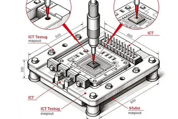
Table of Contents
ICT Test Fixtures: Definition, Structure, and Technical Significance
1.1 What is an ICT Test Fixture?
An ICT test fixture, often called a “bed-of-nails fixture,” is a high-precision mechatronic interface device used to securely physically fixture and electrically connect a PCB to an Automated Test Equipment (ATE) system during testing. Its core structure includes:
- Spring Probe Array: Customized layout based on preset test points on the PCB, enabling multi-point synchronous contact.
- Fixture Baseplate and Alignment Mechanism: Ensures precise alignment between the PCB and the probes.
- Actuation System: Such as pneumatic, vacuum, or mechanical locking mechanisms, providing a reliable clamping force.
1.2 Technical Significance: Early Defect Interception and Economic Impact
The core value of ICT testing lies in its early-stage defect interception capability. Research indicates that performing ICT testing immediately after SMT assembly can identify up to 98% of manufacturing defects, reducing later-stage rework costs by 30–50%. For high-reliability sectors like automotive electronics, medical devices, and aerospace, ICT is a crucial component of a “zero-defect” manufacturing strategy.
Industry Insight: As PCB assembly density increases and components miniaturize (e.g., 01005 packages), manual visual inspection and AOI have limitations in electrical performance verification. ICT, through direct electrical signal measurement, provides irreplaceable verification depth.
How ICT Testing Achieves Four Core Verification Functions
2.1 Component Correct Placement Verification
ICT determines if a component is in the correct location and within specification by measuring its electrical parameters (resistance, capacitance, inductance, etc.). For example:
- Resistor Verification: The test system applies a known current across the component, measures the voltage drop, and calculates the actual resistance.
- Capacitance Verification: Measures the capacitive impedance characteristic using an AC signal.
When measurements fall outside preset tolerance ranges, the system automatically flags “incorrect placement” or “parameter drift,” particularly useful for identifying batch misplacement issues caused by feeder errors.
2.2 Polarity Checking: Key to Mistake-Proofing
Incorrect orientation of polarity-sensitive components (like diodes, electrolytic capacitors, and ICs) can cause circuit shorts, component damage, or even fire risk. ICT performs directional electrical testing for judgment:
- Diode Test: Verifies forward voltage drop (~0.6–0.7V) under forward bias and high impedance under reverse bias.
- Polarized Capacitor Test: Judges installation direction by combining capacitance measurement with leakage current detection.
2.3 Missing Component Detection: Continuity Testing and Parallel Detection Techniques
ICT uses open/short tests to quickly determine component presence. For passive components, missing parts are detected by measuring abnormally high impedance (open) between nodes. For areas with multiple components like integrated circuits, Boundary Scan technology enables large-scale parallel detection, significantly improving test efficiency.
2.4 Solder Joint Quality Assessment: From Electrical Connectivity to Reliability Prediction
Solder joint defects (cold solder joints, insufficient solder, bridging, etc.) are a major cause of intermittent failures. ICT assesses the electrical continuity of solder joints through low-resistance measurement (often using a 4-wire Kelvin detection method):
- Good Solder Joint: Typically exhibits resistance below 0.1Ω.
- Suspicious Solder Joint: Resistance between 0.1–1Ω, potentially indicating micro-cracks or insufficient solder.
- Defective Solder Joint: Excessively high resistance or a complete open circuit.
It’s important to note that while ICT effectively identifies electrical connection defects, it cannot assess the mechanical strength or visual defects of solder joints. Therefore, it is often combined with Automated Optical Inspection (AOI) or Automated X-ray Inspection (AXI) to form a complementary testing strategy.
Types of ICT Test Fixtures and Selection Guide
| Fixture Type | Applicable Scenarios | Advantages | Limitations |
|---|---|---|---|
| Vacuum Fixture | High-density PCBs, Mass Production | High alignment precision, Excellent test consistency | High initial cost, requires vacuum system maintenance |
| Pneumatic Fixture | Medium to High Volume, Fast Test Cycles | Stable clamping, Fast operation speed | Requires an air supply, can be noisy |
| Manual Fixture | Prototype Verification, Low Volume, R&D Debugging | Low cost, High flexibility | Low test efficiency, Operator-dependent |
| Custom Bed-of-Nails Fixture | Complex Boards, High Pin-count Devices | High test coverage, High scalability | Long design lead time, High customization cost |
Selection Recommendations:
- For mass production like automotive electronics, a vacuum fixture with high-density probes is recommended to ensure test stability.
- For multi-variety, low-volume industrial control boards, a modular pneumatic fixture can balance investment and flexibility.
Best Practices for ICT Testing Implementation and Design for Testability (DFT)
4.1 Design for Testability (DFT) Principles
- Provide Test Points: Design test pads with a diameter ≥0.9mm on all critical network nodes.
- Avoid Obstruction: Maintain a 5mm clearance around test points from tall components.
- Isolate Power and Ground: Enable isolated testing of power networks via test pins to improve fault isolation accuracy.
- Incorporate Boundary Scan: Integrate JTAG interfaces for complex ICs (e.g., FPGAs, processors) to enhance controllability and observability.
Process Integration and Data Analysis
- Test Program Generation: Automatically generate test vectors from CAD data to reduce programming time.
- Data Traceability: Link ICT test results with production lots and component batches for quality traceability.
- Trend Analysis: Use Statistical Process Control (SPC) to identify process drifts (e.g., solder paste printing issues, reflow profile anomalies).
Technical Challenges and Future Evolution
5.1 Current Challenges
- Miniaturization Limits: Increasing difficulty of physical probe contact as package sizes shrink below 0201.
- High-Frequency Testing Limitations: Electrical testing of RF circuits (>1GHz) requires specialized impedance-matching designs.
- Flexible Board Testing: Higher demands for alignment and contact stability for Flexible Printed Circuits (FPC).
5.2 Technological Trends
- Non-Contact Testing Technologies: Combining technologies like Flying Probe testing with ICT to adapt to high-mix production.
- Intelligent Fixtures: Integrating sensors for real-time monitoring of probe pressure and contact resistance, enabling predictive maintenance.
- Data-Fusion Testing: Using AI to amalgamate ICT data with AOI, AXI, and functional test results for a comprehensive quality profile.
Conclusion
ICT test fixtures are not merely inspection tools but the carriers of a systems engineering approach spanning design, manufacturing, and quality management. Through precise electrical verification, they ensure zero placement errors, zero reversed polarities, and zero solder defects, fundamentally enhancing PCBA reliability. Amidst the advancement of smart factories and Industry 4.0, ICT is deeply integrating with IoT and big data analytics, evolving from “defect detection” towards “process optimization and prediction.”
For enterprises pursuing manufacturing excellence, investing in advanced ICT testing solutions is not only a quality assurance measure but a core strategy for enhancing market competitiveness and reducing total lifecycle costs.
Challenges and Countermeasures for ICT Test Fixtures
Core Conflict: High initial investment vs. long-term returns.
Solution: Conduct a Total Cost of Ownership (TCO) analysis, quantifying the avoided costs of late-stage rework, scrap, and reputation damage through early defect interception. Start with a pilot on a small batch of critical products to demonstrate ROI with data.
A: Core Conflict: High-density, miniaturized PCB designs vs. the need for physical probe contact.
Solution: Integrate Design for Testability (DFT) early in the PCB layout phase, mandating test point placement. Utilize micro-probes, Boundary Scan (JTAG), or supplement with Flying Probe Testing.
A: Core Conflict: Complex, time-consuming programming vs. the need for rapid adaptation to design changes.
Solution: Leverage software to auto-generate test program frameworks from design files, establish a library of standard component tests, and implement strict version control for programs.
A: Core Conflict: Probes are consumables vs. the requirement for stable, reliable test results.
Solution: Implement a Preventive Maintenance Schedule: daily cleaning, regular servicing, periodic calibration, and maintaining a stock of critical spare parts.
A: Core Conflict: ICT excels at electrical testing vs. its inability to detect functional, visual, and hidden defects.
Solution: Build a Combinatorial Test Strategy, integrating ICT with SPI, AOI, AXI, and FCT to form a complementary “Test Pyramid” for comprehensive coverage.