O fabrico de PCB é um processo em várias etapas, rigorosamente controlado onde pequenos desvios podem levar a problemas de fiabilidade, perda de rendimento ou aumento de custos.
Embora muitos recursos descrevam o fabrico de PCB a um nível elevado, a compreensão a forma como cada etapa de fabrico interage com a seguinte é fundamental para:
- Conceção de placas susceptíveis de serem fabricadas
- Controlo dos custos
- Garantir a fiabilidade a longo prazo
Este artigo fornece uma visão geral passo a passo do processo de fabrico de PCBcom ligações para explicações pormenorizadas de cada fase crítica.
A perspetiva reflecte práticas de fabrico reais utilizadas por fabricantes profissionais de PCB, tais como TOPFASTA empresa é uma das maiores empresas do mundo, onde a estabilidade do processo e o controlo do rendimento são as principais prioridades.
Índice
Visão geral do Processo de fabrico de PCB
Um fluxo de trabalho típico de fabrico de PCB inclui:
- Fabrico da camada interior
- Perfuração (mecânica ou a laser)
- Revestimento de cobre
- Gravura de padrão
- Inspeção e controlo do rendimento
Cada etapa baseia-se na anterior. Os erros cometidos no início do processo muitas vezes não podem ser corrigidos mais tarde.
Fabrico da camada interior
O fabrico da camada interior é o fundamentos do fabrico de PCB multicamadas.
Nesta fase:
- A folha de cobre é modelada para formar circuitos internos
- A precisão dimensional é fundamental
- Os defeitos ficam permanentemente bloqueados na pilha após a laminação
Uma vez que as camadas interiores não podem ser reparadas depois de laminadas, os fabricantes aplicam controlos de processo e normas de inspeção rigorosos.
Para uma explicação pormenorizada da preparação da camada interna, imagiologia e gravação, ver:
Explicação do fabrico da camada interior
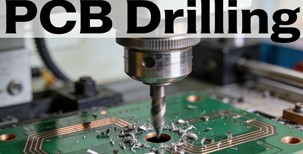
Perfuração de PCB: Criando conexões entre camadas
A perfuração cria os orifícios que mais tarde se tornarão vias e ligações através de orifícios.
São utilizados dois métodos principais de perfuração:
- Perfuração mecânica
- Perfuração a laser
Cada método tem contrapartidas:
- Tamanho do furo
- Rácio de aspeto
- Custo
- Fiabilidade
A perfuração incorrecta afecta diretamente a qualidade do revestimento e a fiabilidade da via.
Para saber quando é que a perfuração mecânica ou a perfuração a laser é adequada, leia:
Perfuração de PCB vs. Perfuração a laser
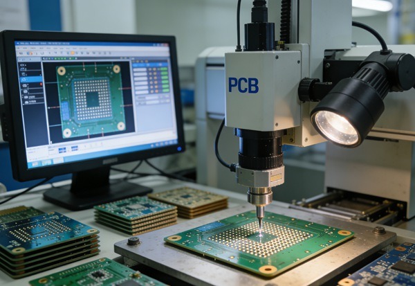
Processo de revestimento de cobre
O revestimento de cobre transforma os orifícios perfurados em ligações verticais condutoras de eletricidade.
O processo de revestimento inclui:
- Deposição de cobre sem eletrólise
- Acumulação de espessura de cobre eletrolítico
A qualidade do revestimento é determinada:
- Via resistência da parede
- Desempenho em ciclos térmicos
- Capacidade de transporte de corrente
O revestimento inconsistente é uma causa comum de falhas no terreno, mesmo quando as placas passam nos testes eléctricos iniciais.
Para uma análise completa das fases de revestimento e considerações de fiabilidade, ver:
Explicação do processo de revestimento de cobre no fabrico de PCB
Gravação de PCB e formação de circuitos
A gravação remove o cobre não desejado para definir o padrão final do circuito.
Esta etapa deve ser equilibrada:
- Espessura do cobre
- Precisão da largura da linha
- Controlo do espaçamento
A sobrecondicionamento ou subcondicionamento conduz a:
- Abre ou calça
- Variação da impedância
- Redução do rendimento de fabrico
O desempenho da gravação torna-se cada vez mais crítico à medida que os projectos avançam para traços mais finos e contagens de camadas mais elevadas.
Para uma análise aprofundada da química da gravação e do impacto no rendimento, leia:
Explicação do processo de gravação de PCB e do controlo de rendimento
Controlo do rendimento em todo o processo de fabrico
O rendimento não é controlado numa única etapa - é o resultado da estabilidade cumulativa do processo.
Os principais factores de rendimento incluem:
- Precisão da camada interior
- Qualidade da broca
- Uniformidade da galvanização
- Consistência da gravura
Os fabricantes profissionais de PCB monitorizam continuamente os dados de rendimento para:
- Identificar a deriva do processo
- Otimizar as regras de conceção
- Reduzir o desperdício e o retrabalho
Na TOPFAST, o feedback de rendimento é integrado nas revisões DFM para ajudar os clientes a evitar riscos de fabrico ocultos antes do início da produção.
Para uma visão geral dos factores de rendimento centrada na indústria transformadora, ver:
Explicação do processo de gravação de PCB e do controlo de rendimento
Como as decisões de conceção afectam o processo de fabrico
Do ponto de vista do fabrico, muitos problemas de PCB têm origem em escolhas de design como:
- Larguras de traço excessivamente finas
- Vias de elevado rácio de aspeto
- Distribuição de cobre não equilibrada
- Tolerâncias demasiado apertadas
A colaboração precoce entre projectistas e fabricantes ajuda a alinhar a intenção do projeto com a capacidade do processo.
Esta abordagem reduz:
- Iterações
- Atrasos na produção
- Custo total de propriedade
Perspetiva do fabricante: Integração de processos na TOPFAST
Como fabricante profissional de PCB, a TOPFAST aborda o fabrico de PCB como um sistema integradoe não passos isolados.
Os princípios fundamentais incluem:
- Janelas de processo estáveis
- Identificação precoce dos riscos de DFM
- Otimização orientada para o rendimento
- Normas de qualidade alinhadas com o IPC
Em vez de se concentrar apenas nas especificações mínimas, a ênfase é colocada em repetibilidade, fiabilidade e produção escalável.
Conclusão
O processo de fabrico de PCB é uma sequência de etapas interdependentes em que a qualidade é construída progressivamente e não inspeccionada no final.
Ao compreender como o fabrico da camada interna, a perfuração, o revestimento de cobre e a gravação funcionam em conjunto, os engenheiros e os compradores podem:
- Tomar melhores decisões de conceção
- Reduzir o risco de fabrico
- Controlo de custos sem sacrificar a qualidade
Esta visão geral serve de porta de entrada para explicações técnicas mais aprofundadas de cada fase crítica, reflectindo práticas do mundo real utilizadas por fabricantes de PCB experientes, como TOPFAST.