This article delves into the complex systems engineering involved in conductor spacing calculations for high-voltage printed circuit board (PCB) design. Moving beyond foundational safety standards, it analyzes the underlying logic of spacing design from multiple dimensions, including materials science, failure mechanisms, and environmental dynamics, providing forward-looking guidance for high-voltage PCB reliability design.
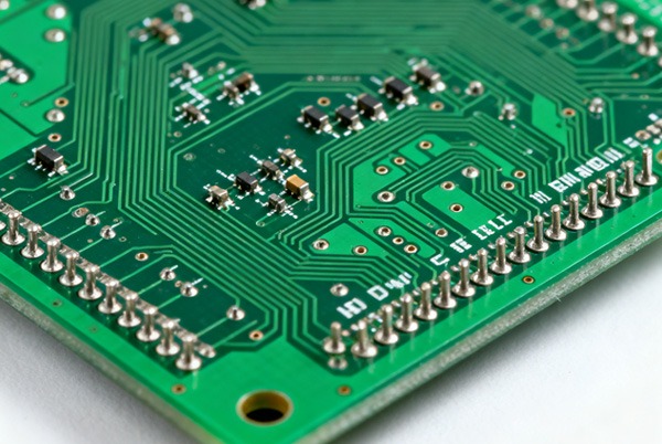
Table of Contents
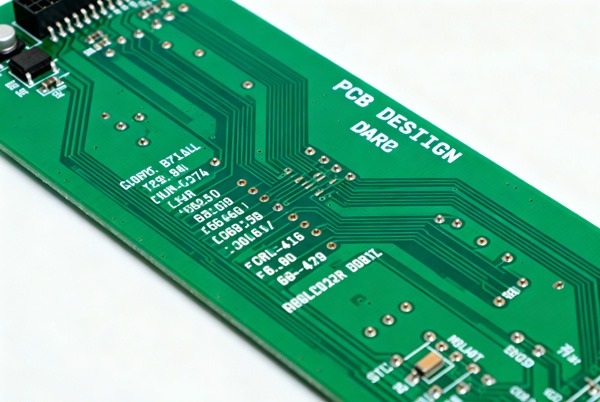
Conductor Spacing Design
High-voltage PCB design has evolved from mere compliance with standards to a complex systems engineering discipline requiring a deep understanding of electric field distribution, material interface behavior, and environmental coupling effects. When operating voltages exceed 30V AC / 60V DC, conductor spacing design is no longer just a matter of “safe distance”; it becomes an optimization challenge involving multi-physics coupling.
1.1 The Duality of Spacing Parameters
- Clearance: The shortest path through air, governed primarily by Paschen’s Law, exhibiting a complex non-linear relationship with air pressure, humidity, and temperature.
- Creepage Distance: The path along an insulating surface, influenced by interface phenomena such as surface resistivity, wettability, and contamination accumulation.
- Key Insight: For the same numerical distance, the reliability of a creepage path is typically lower than that of an air gap, due to the time-varying nature of surface conditions.
The Materials Science Perspective
The Comparative Tracking Index (CTI) is often simplified as a material “grade label,” but it fundamentally reflects the structural stability of polymer substrates under electric fields.
2.1 The Microscopic Mechanism of CTI
- Electrochemical Dendrite Formation: CTI testing essentially evaluates a material’s resistance to electrochemical dendritic crystal growth.
- Thermal-Electrical Coupling Effect: High CTI materials typically exhibit better thermal conductivity and a higher glass transition temperature (Tg), enabling the faster dissipation of local hot spots.
- Material Matching Principle: When CTI < 200, for each drop in classification level, the required creepage distance should increase by 15-20%—an empirical rule not explicitly quantified in standards.
2.2 Development of Advanced Substrates
- High-Frequency, High-Voltage Composite Materials: PTFE/ceramic-filled materials with CTI > 600, combining low loss and high arc resistance.
- Nano-Modified Epoxy Resins: Doped with SiO₂/Al₂O₃ nanoparticles, improving mechanical strength while increasing CTI by 30-50%.
In-Depth Failure Mechanism Analysis
3.1 Multi-Factor Coupling Model for Conductive Anodic Filament (CAF) Growth
Recent research indicates that CAF formation is the result of a tripartite interaction between electrochemical, mechanical stress, and thermal aging:
CAF Growth Rate = f(Electric Field Strength) × g(Temperature) × h(Humidity) × φ(Mechanical Stress)Where the electric field strength has an exponential relationship, and for every 10°C temperature increase, CAF risk increases 2-3 fold.
3.2 Dynamic Evolution of Surface Contamination
Pollution Degree is not a static parameter but a function of time:
- Dust + Humidity Synergistic Effect: When relative humidity > 60%, the resistivity of ordinary dust can drop by 3-4 orders of magnitude.
- Ion Migration Dynamics: Under DC bias, ions like Na⁺ and Cl⁻ can migrate at speeds of 0.1–1 μm/s, rapidly forming conductive channels.
A Hierarchical Design Framework for High-Voltage Insulation Systems
4.1 Engineering Implementation of the Five-Level Insulation System
| Insulation Class | Core Requirement | Spacing Multiplier | Application Scenario |
|---|---|---|---|
| Basic Insulation | Single fault protection | 1.0 | Inside the Class I equipment |
| Supplementary Insulation | Redundant protective layer | 1.2–1.5 | Critical safety areas |
| Double Insulation | Independent dual systems | 1.8–2.0 | Hand-held equipment |
| Reinforced Insulation | Single-layer equivalent to double | 2.0–2.5 | Medical/Aerospace |
| Functional Insulation | Performance requirement only | 0.6–0.8 | Between SELV circuits |
4.2 The Deeper Role of Conformal Coatings
- Electric Field Homogenization Effect: Coatings with a high dielectric constant (εᵣ > 4.5) can reduce the surface electric field gradient by 30-40%.
- Volume Resistivity vs. Surface Resistivity: High-quality parylene coatings have volume resistivity > 10¹⁶ Ω·cm, but surface contamination can still create bypass paths.
- “Amplification Effect” of Coating Defects: Electric field strength at pinhole defects can increase 10-100 times, triggering local breakdown.
A Dynamic Correction Model for Spacing Calculation
The look-up table method in standards has limitations, necessitating the introduction of dynamic correction factors:
5.1 The Physical Basis of Altitude Correction
For every 1000m increase in altitude, air breakdown voltage decreases by approximately 10%, but nonlinearly:
Correction Factor Kₐ = e^(h/8150) (where h is altitude in meters)In practice, at 2000m altitude, clearance needs to increase by 15-20%.
5.2 Statistical Consideration of Transient Overvoltages
- Lightning Surge: For 1.2/50μs waveforms, requiring instantaneous withstand capability to be 2-4 times higher.
- Switching Surge: In power electronic equipment, when dv/dt > 1000 V/μs, displacement current effects must be considered.
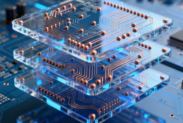
Advanced Topology Techniques for High-Density, High-Voltage PCBs
6.1 3D Creepage Distance Optimization
Effective Creepage Ratio = (Actual Surface Path) / (Straight-Line Distance)- V-Groove Optimization: When groove depth-to-width ratio > 1.5, effective creepage ratio can reach 2.0–3.0.
- Vertical Isolation Walls: FR4 walls with a thickness of> 0.8mm can withstand 8–10 kV/mm.
6.2 Gradient Design for Mixed-Voltage PCBs
- Electric Field Gradient Control: Voltage difference between adjacent conductors should transition smoothly, avoiding abrupt changes > 300 V/mm.
- Protected Zone Layout: Establish 2–3mm “copper-free zones” between high and low voltage areas, filled with protective dielectric material.
Standard Evolution and Future Trends
7.1 Supplements from Emerging Standards
- IEC 62368-1: Replaces 60950-1, introducing the concept of energy source classification.
- IPC-9592: Specific requirements for power converters, focusing on thermal-electrical synergistic failures.
7.2 Simulation-Driven Spacing Design
- Finite Element Electric Field Simulation: Identifies electric field concentration areas, optimizing to save 20-30% space compared to standard methods.
- Multi-Physics Coupling Analysis: Combined electrical-thermal-mechanical stress simulation to predict long-term reliability.
Design Verification and Reliability Assessment Framework
8.1 Accelerated Testing Strategy
- Temperature Humidity Bias (THB) Testing: 85°C / 85% RH / Rated Voltage, assessing insulation resistance decay rate.
- Step-Stress Testing: Voltage increased in 10-20% steps to identify soft breakdown thresholds.
8.2 Online Monitoring Technologies
- Partial Discharge Detection: Detects discharge levels in the pC range, providing early warning of insulation degradation.
- Online Insulation Resistance Monitoring: Real-time monitoring of GΩ-level resistance.
Conclusion
High-voltage PCB spacing design is undergoing a paradigm shift from empirical rules to model-based prediction, and onward to intelligent optimization. Future directions include:
- Material Database & AI Matching: Automatically recommending substrate materials and spacing based on operating conditions.
- Digital Twin Verification: Virtual prototypes validate spacing rationality through multiphysics simulation.
- Adaptive Design: Dynamically adjusting operating parameters based on sensor feedback to compensate for insulation aging.
Design engineers must establish a systems-level safety perspective, unifying spacing design with considerations for thermal management, mechanical structure, and environmental protection. By achieving a deep understanding of failure physics rather than simply adhering to standards, the reliable operation of high-voltage electronic products in increasingly harsh environments can be achieved.