2026 Switzerland PCB Manufacturing: The Gold Standard of Precision
PCB Manufacturing
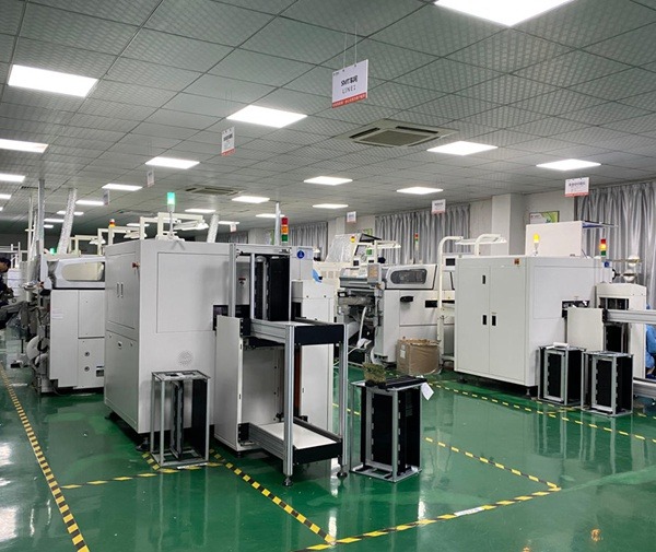
PCB Manufacturer
Switzerland is synonymous with precision engineering and world-leading medical innovation. This guide explores the Swiss PCB ecosystem, focusing on the rigorous quality standards required for the MedTech and Aerospace sectors, and how Swiss engineering firms can leverage TopFast’s advanced HDI capabilities to maintain their competitive edge in 2026.