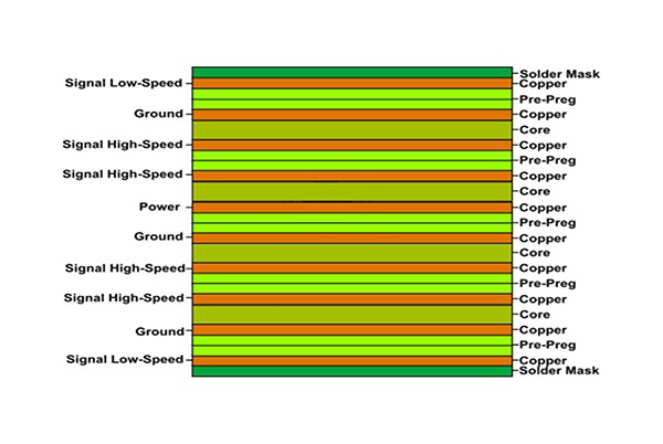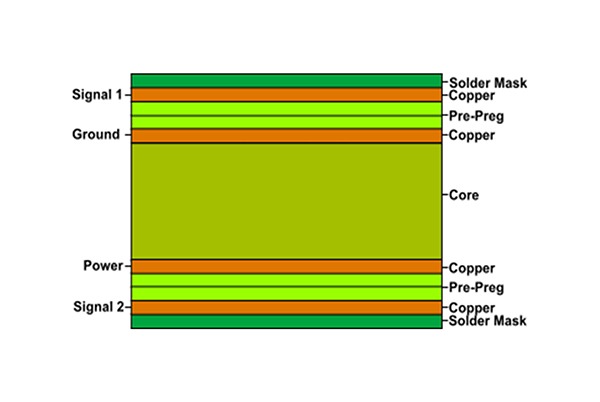
4-layer 1.6 mm PCB laminate structure
The laminate structure of a 4-layer 1.6 mm PCB is analyzed, focusing on the advantages of this standard thickness PCB in terms of impedance control, signal integrity, and EMC. At the same time, the application scenarios of 4-layer boards of different thicknesses are compared, and professional manufacturing process analysis is provided.