Join Topfast at ExpoElectronica 2026: Discover Leading PCB & Electronic Component Solutions in Moscow
Heading to Moscow for ExpoElectronica 2026? Stop by Topfast at Booth C3111 (Pavilion 3) from…
Read Article →Advanced ceramic substrates for high-power, high-frequency, and extreme environment applications
Get Instant QuoteOur commitment to excellence through international quality standards
Class 3 Performance
Quality Management System
Restriction of Hazardous Substances
Flammability Rating
Aerospace Quality Management
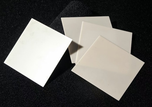
Advanced ceramic PCB technologies for demanding applications
Most common ceramic substrate with excellent thermal and electrical properties.
Superior thermal conductivity ceramic for high-power applications.
Highest thermal conductivity ceramic for extreme thermal management.
Multilayer ceramic technology for high-frequency and 3D integration.
Key properties of different ceramic substrate materials
Specialized manufacturing processes for ceramic circuit boards
Precision cutting and surface preparation of ceramic substrates with laser or diamond tools.
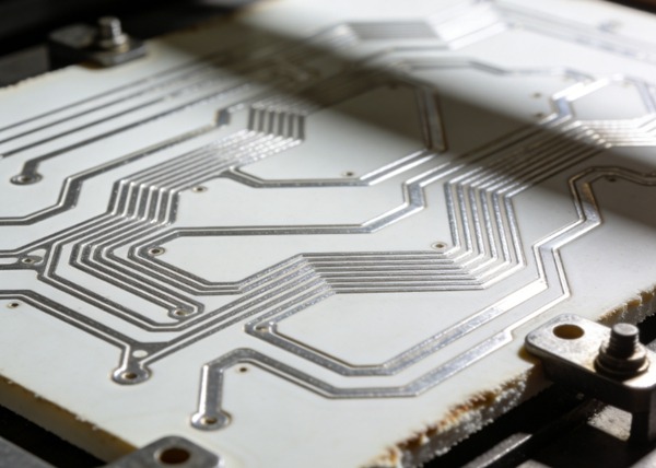
Thick film or thin film metallization processes using screen printing, sputtering, or plating.
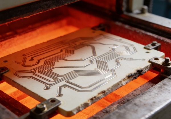
High-temperature firing in controlled atmosphere furnaces to bond metallization layers.
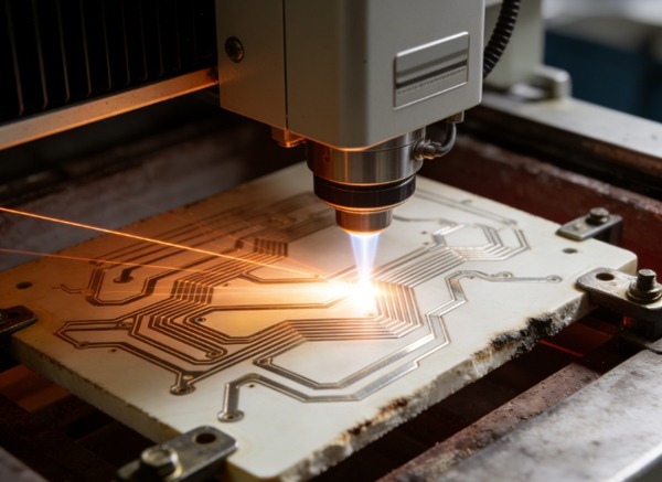
Precision laser cutting, drilling, and scribing for vias, cavities, and final dimensions.
Our manufacturing capabilities for ceramic PCB production
Minimum trace width on ceramic
Minimum trace spacing
Minimum via diameter
Minimum via center spacing
Available ceramic thickness
Key advantages over traditional PCB materials
Superior heat dissipation (10-20x better than FR-4)
Stable performance from -55°C to +850°C
High dielectric strength and low loss
High flexural strength and rigidity
Resistant to solvents, acids, and bases
Advanced ceramic PCB manufacturing for extreme applications
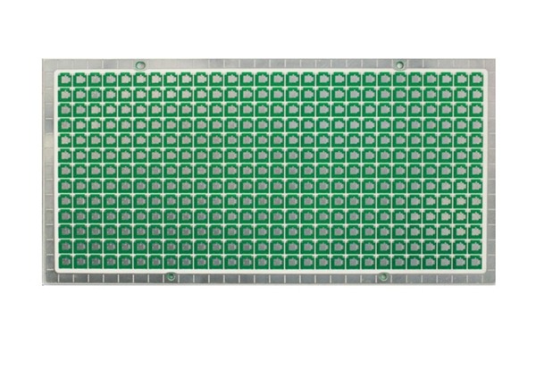
Power Lighting PCBs are printed circuit boards (PCBs) used in power and lighting equipment
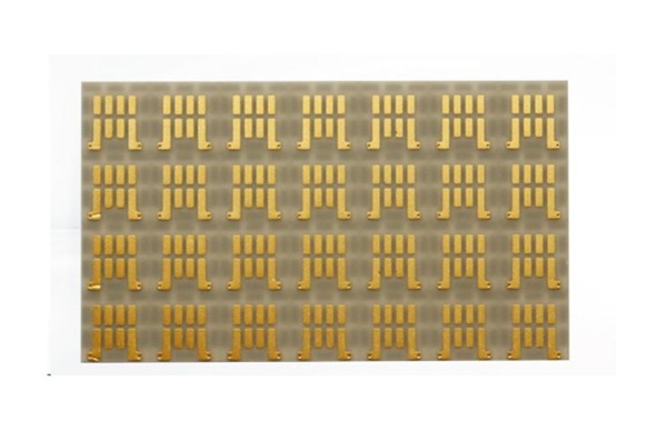
Deep Ultraviolet (DUV) purifier PCBs are specialized circuit boards designed to power and control UV-C disinfection…
All of our products are IPC rated with ISO 14001; ISO 9001; CE; ROHS certificates, etc. Our products are widely used in communication, medical equipment, industrial control, power supply, consumer electronics and aerospace, automotive industry and other fields.
According to the different needs, different processes, our factory can do ceramic circuit boards, can do the traditional process layer 2-8 layers, using low temperature co-fired ceramic (LTCC) and high temperature co-fired ceramic (HTCC), can reach 10-20 layers, or even higher. In actual application we will choose according to the customer, the type of process required and demand.
Using the common ceramic circuit board thick film process, it is an advanced printed circuit board manufacturing technology with the advantages of easy multi-layer wiring, low cost, high temperature resistance, corrosion resistance, good mechanical strength, etc., which is widely used in the fields of electronics, communications, aerospace and so on.
We can't produce without gerber file, we produce based on Gerber. Or if you have any samples, we can also clone based on the samples, if so, we can send 3-5 samples to our company, and then evaluate the price of making samples for you.
The fastest delivery time we can support is 12 hours. 1 hour for prompt quotation. 4 hours for prompt engineering. This depends on your product requirements and quantity. In addition, lead time will be included in your quote.
As a global PCB manufacturer, our factories are located in Guangzhou, China and Shenzhen, China, utilizing the strengths of each region to best serve you.
Technical articles and industry knowledge about ceramic PCB technology
Heading to Moscow for ExpoElectronica 2026? Stop by Topfast at Booth C3111 (Pavilion 3) from…
Read Article →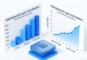
The selection of PCB materials and layer stackup is a core factor affecting manufacturing costs.…
Read Article →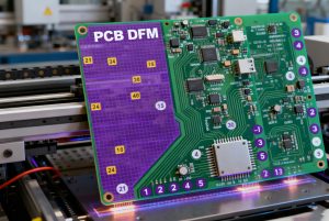
This comprehensive guide covers essential PCB DFM principles including layout specifications, component spacing requirements, and…
Read Article →Get expert consultation and instant quote with free ceramic material selection guidance