Gruppo PCB (PCBA) è la fase in cui un Il PCB nudo si trasforma in una scheda elettronica funzionaleLa fabbricazione di PCB si concentra sulla fase di produzione della scheda nuda, che costituisce la base dell'intero flusso di lavoro di produzione dei PCB. Comprende posizionamento dei componenti, saldatura e test rigorosi
La qualità dell'assemblaggio influisce direttamente:
- Funzionalità elettrica
- Affidabilità del prodotto
- Rendimento di produzione
A TOPFAST, l'assemblaggio è trattato come un processo guidato dal rendimentoassicurando che le schede siano funzionali e robuste.
Per informazioni su come l'assemblaggio dei PCB sia collegato alla fabbricazione, si veda: Fabbricazione di PCB e assemblaggio di PCB
Indice per materie
Tecnologia di montaggio in superficie (SMT) Montaggio
Che cos'è l'assemblaggio SMT?
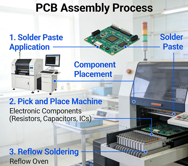
L'assemblaggio SMT prevede il montaggio componenti a montaggio superficiale direttamente sulle piazzole del PCB:
- Pasta saldante
- Macchine pick-and-place
- Saldatura a riflusso
SMT è veloce, preciso e adatto a schede ad alta densitàcomunemente utilizzati nell'elettronica di consumo, nelle telecomunicazioni e nei dispositivi IoT.
Sfide SMT
- I componenti a passo fine richiedono un'estrema precisione di posizionamento
- Lo stress termico durante la rifusione può danneggiare i PCB se gli strati interni o la placcatura in rame non sono coerenti.
- I pannelli ad alta densità aumentano la sensibilità alla resa
In TOPFAST, l'assemblaggio SMT è accuratamente coordinato con i dati di fabbricazione per ridurre al minimo i difetti e migliorare la resa.
Montaggio con foro passante
Che cos'è il montaggio a foro passante?
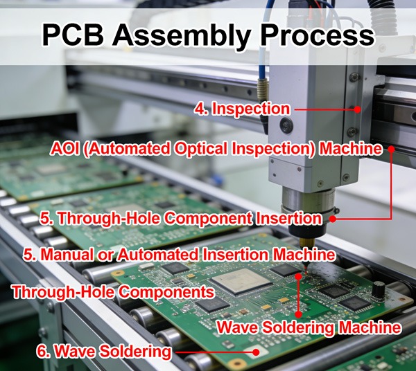
L'assemblaggio a foro passante inserisce i componenti con i conduttori nei fori e li salda:
- Saldatura a onda (saldatura di massa)
- Saldatura manuale (per prototipi o schede a basso volume)
Il foro passante è ancora ampiamente utilizzato per:
- Resistenza meccanica
- Componenti ad alta potenza
- Connettori e pacchetti di grandi dimensioni
Flusso di lavoro per l'assemblaggio del foro passante
- Riempimento di fori / Inserimento di componenti - Inserire i conduttori dei componenti nei fori placcati
- brasatura - La saldatura a onda o selettiva fissa i componenti
- Ispezione - Controlli visivi o AOI per la qualità della saldatura
La qualità della foratura e della placcatura è direttamente influenzata da Foratura di PCB vs foratura laser, e Spiegazione del processo di ramatura.
Sfide per i fori passanti
- Fori disallineati o mal placcati riducono l'affidabilità del giunto di saldatura
- L'assemblaggio manuale aumenta il costo della manodopera e il potenziale di errore umano.
- Richiede più spazio sulla scheda rispetto all'SMT
TOPFAST combina foratura e placcatura di precisione con ottimizzazione dell'assemblaggio per massimizzare la resa dei fori passanti.
Test e controllo qualità nell'assemblaggio
Test in-circuit (ICT)
Controlli TIC
- Pantaloncini
- Apre
- Valori corretti dei componenti
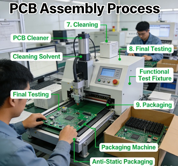
Test funzionali
Il test funzionale simula il funzionamento reale per verificare che la scheda funzioni come progettato.
Il collaudo è il punto di controllo finale che assicura che le fasi di fabbricazione e assemblaggio siano conformi alle specifiche. Vedere Spiegazione del processo di incisione e del controllo della resa per capire come la qualità delle fasi iniziali influisca sui risultati dei test.
Considerazioni sulla resa dell'assemblaggio
Rendimento
- Qualità della fabbricazione (ad es. strati interni, foratura, placcatura)
- Precisione di posizionamento dei componenti
- Parametri di saldatura
- Progettazione della scheda (termica, spaziatura, dimensioni dei pad)
L'assemblaggio ad alto rendimento riduce:
- Rielaborazione
- Rottami
- Costo di produzione complessivo
- Fare riferimento a Fabbricazione di PCB e assemblaggio di PCB per capire come le considerazioni sulla resa riguardino entrambi i processi.
Fattori di costo nell'assemblaggio
I principali fattori di costo:
- Tipo di componente e confezione
- Densità del pannello e numero di strati
- Volume di assemblaggio (prototipo o produzione di massa)
- Requisiti per i test e le ispezioni
Ottimizzare l'assemblaggio senza sacrificare la qualità richiede stretto allineamento tra i processi di progettazione, fabbricazione e assemblaggio.
conclusioni
L'assemblaggio di PCB trasforma una scheda nuda in un prodotto elettronico completamente funzionale.
Processi SMT e a foro passante, combinati con test robusti, definiscono l'affidabilità del prodotto finale.
L'integrazione con la qualità della fabbricazione è essenziale da raggiungere:
- Alto rendimento
- Produzione efficiente dal punto di vista dei costi
- Affidabilità a lungo termine
FAQ sul processo di assemblaggio dei PCB
R: L'assemblaggio dei circuiti stampati prevede il montaggio dei componenti elettronici su un circuito stampato fabbricato con tecniche SMT o a foro passante, seguito da ispezione e collaudo.
R: L'SMT monta i componenti sulla superficie del PCB, mentre il foro passante inserisce i conduttori dei componenti nei fori e li salda.
R: Strati non allineati, fori non correttamente eseguiti o placcature non uniformi possono causare difetti di saldatura e ridurre la resa dell'assemblaggio.
R: Si utilizzano comunemente l'ispezione ottica automatizzata (AOI), l'ispezione a raggi X, i test in-circuit (ICT) e i test funzionali.
R: TOPFAST allinea i processi di fabbricazione e assemblaggio, applica ispezioni automatiche e manuali e utilizza l'ottimizzazione della resa per una produzione affidabile.