L'incisione è il processo che trasforma il rame placcato in precisi schemi di circuito.
Anche se all'apparenza sembra semplice, l'incisione è uno dei metodi di le fasi più sensibili alla resa nella produzione di PCB.
Dal punto di vista del produttore, un controllo insufficiente dell'incisione porta a..:
- Variazione della larghezza della linea
- Pantaloncini e aperture
- Basso rendimento
- Costi di produzione più elevati
Questo articolo spiega come funziona l'incisione dei PCB, cosa influisce sulla qualità dell'incisione e come i produttori come TOPFAST controllare la resa per garantire una produzione di PCB costante ed economicamente vantaggiosa.
Indice per materie
Che cos'è l'incisione dei PCB?
L'incisione dei PCB è un processo chimico che rimuove il rame indesiderato dalla scheda, lasciando solo il circuito progettato.
L'incisione viene applicata a:
- Strati interni
- Strati esterni
L'obiettivo è quello di raggiungere larghezza, spaziatura e geometria delle tracce accurate secondo le specifiche di progetto.
Tipi di processi di incisione dei PCB
Incisione dello strato interno
Si verifica l'incisione dello strato interno:
- Prima della laminazione
- Su un sottile foglio di rame
È altamente sensibile perché:
- I difetti non possono essere riparati dopo la laminazione
- La resa dello strato interno influisce sull'intero stack di PCB
Incisione dello strato esterno
Si verifica l'incisione dello strato esterno:
- Dopo la ramatura
- Su strati di rame più spessi
L'incisione dello strato esterno deve tenere conto di:
- Spessore del rame placcato
- Uniformità su tutto il pannello
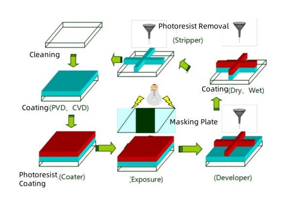
Processo di incisione dei PCB passo dopo passo
Fase 1 - Preparazione del modello di resistenza
Uno strato di resistenza protegge le aree di rame che dovrebbero rimanere dopo l'incisione.
La precisione del modello in questa fase determina la geometria finale della traccia.
Fase 2 - Mordenzatura chimica
Le soluzioni chimiche rimuovono selettivamente il rame esposto.
Variabili chiave del processo:
- Concentrazione del mordente
- Temperatura
- Pressione di spruzzo
- Tempo di mordenzatura
Il controllo di queste variabili è essenziale per ottenere risultati stabili.
Fase 3 - Spelatura delle resistenze
Dopo l'incisione, la resistenza rimanente viene rimossa, rivelando le tracce di rame finite.
Difetti di incisione comuni e loro impatto
Sovraincisione
Cause:
- Tempo di incisione eccessivo
- Chimica aggressiva
Risultati:
- Larghezza di traccia ridotta
- Aumento dell'impedenza
- Potenziale apertura
Sottoincisione
Cause:
- Tempo di incisione insufficiente
- Attività mordenzante debole
Risultati:
- Rame residuo
- Corti tra le tracce
Sottotaglio
Il mordenzante rimuove il rame lateralmente sotto la resistenza, riducendo la larghezza della traccia.
Il sottosquadro diventa più grave con:
- Rame più spesso
- Tracce più fini
Che cos'è la resa nella produzione di PCB?
Il rendimento si riferisce alla percentuale di schede conformi alle specifiche dopo la produzione.
Alto rendimento significa:
- Costo unitario inferiore
- Qualità stabile
- Consegna prevedibile
Il basso rendimento porta a:
- Rottami
- Rielaborazione
- Costo complessivo più elevato
Come l'incisione influisce sulla resa di produzione
L'incisione ha un impatto diretto sulla resa perché:
- I difetti di traccia causano guasti elettrici
- I difetti dello strato interno si moltiplicano tra i pannelli
- Piccole variazioni influenzano i progetti ad alta densità
Dal punto di vista del produttore, l'incisione è una delle punti di leva più alti per il miglioramento della resa.
Fattori di progettazione che influenzano la resa dell'incisione
La resa migliora quando si progetta:
- Evitare tracce inutilmente sottili
- Mantenere una larghezza di linea coerente
- Equilibrio della distribuzione del rame
- Utilizzare la distanza minima raccomandata dal produttore
DFM spesso rivela precocemente i rischi legati all'incisione.
Come i produttori controllano la resa dell'incisione
Monitoraggio del processo
I controlli chiave includono:
- Analisi chimica continua
- Calibrazione delle apparecchiature
- Misura della larghezza della linea in tempo reale
Ottimizzazione a livello di pannello
I produttori ottimizzano:
- Layout del pannello
- Bilancio del rame
- Uniformità dell'incisione sul pannello
Ispezione e feedback
AOI e i test elettrici forniscono un feedback a:
- Regolare i parametri di incisione
- Migliorare la stabilità del processo
In TOPFAST, i dati sulla resa vengono utilizzati attivamente per perfezionare i processi di incisione e prevenire problemi ripetuti.
Impatto sui costi dell'incisione e della perdita di rendimento
Il basso rendimento aumenta i costi a causa di:
- Materiali di scarto
- Manodopera aggiuntiva
- Ritardi nella produzione
Migliorare la resa di incisione è spesso più efficace che costo del materiale da taglio quando si riduce il prezzo dei PCB.
Il punto di vista del produttore: La strategia di incisione guidata dal rendimento di TOPFAST
TOPFAST controlla la resa di incisione attraverso:
- Finestre di processo standardizzate
- Raccomandazioni di progettazione conservativa
- Feedback iniziale del DFM
- Monitoraggio continuo della resa
L'attenzione è rivolta a qualità costante e produzione scalabilenon solo di rispettare le tolleranze minime.
conclusioni
L'incisione dei circuiti stampati è un processo ingannevolmente semplice con una un forte impatto sulla resa, sui costi e sull'affidabilità.
Comprendendo come funziona l'incisione e cosa influisce sulla resa, progettisti e acquirenti possono prendere decisioni più intelligenti:
- Ridurre il rischio di produzione
- Costo totale inferiore
- Migliorare l'affidabilità del prodotto
Con un approccio produttivo orientato al rendimento, TOPFAST garantisce una qualità di incisione stabile che supporta una produzione affidabile di PCB su scala..
Lettura correlata
Processo di produzione dei PCB Processo di produzione dei PCB
Realizzazione dello strato interno del PCB
Foratura di PCB vs foratura laser
Processo di placcatura del rame
Controllo della resa dell'acquaforte FAQ
R: L'incisione dei circuiti stampati è un processo chimico che rimuove il rame indesiderato per formare modelli di circuiti.
R: La sovraincisione è causata da un tempo di incisione eccessivo o da soluzioni chimiche troppo aggressive.
R: Uno scarso controllo dell'incisione porta a difetti di traccia, riducendo la resa e aumentando i costi.
R: Sì. I progetti con tracce di larghezza e spaziatura ragionevoli migliorano significativamente la resa dell'incisione.
R: TOPFAST utilizza processi standardizzati, monitoraggio in tempo reale e feedback DFM per mantenere stabile la resa di incisione.