Description
Table of Contents
Product Overview
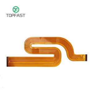
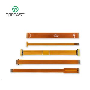
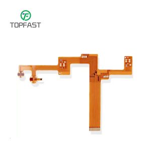
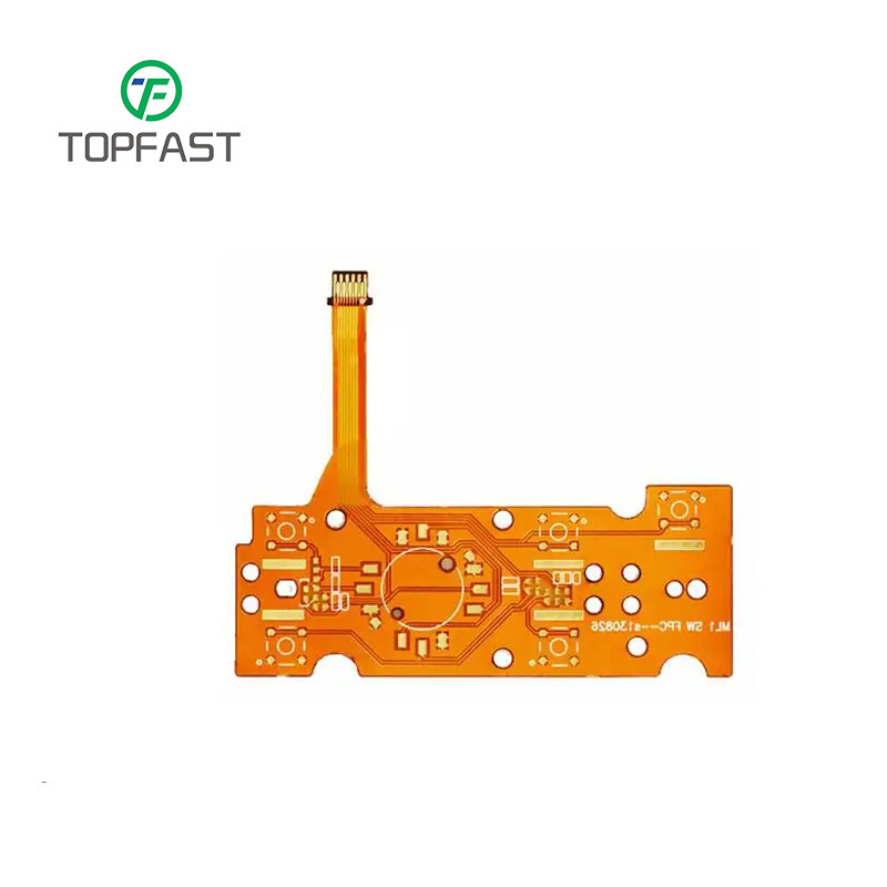
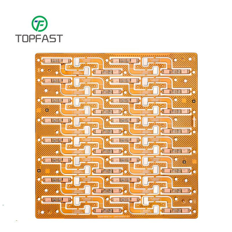
Multilayer Flexible Printed Circuit Boards (Multilayer FPCs) are high-performance interconnect components composed of alternating layers of flexible substrates and conductive copper. Compared to single/double-sided FPCs, multilayer FPCs enable more complex circuit designs through interlayer connections (e.g., laser drilling, plated through-holes), making them suitable for high-density, high-reliability electronic devices.
Multilayer FPCs are widely used in consumer electronics, automotive electronics, medical devices, aerospace, and 5G communications, meeting demands for miniaturization, lightweight design, and bendability.
Flexible PCB Parameters
| Item | Flexible PCB |
| Max Layer | 8L |
| Inner Layer Min Trace/Space | 3/3mil |
| Out Layer Min Trace/Space | 3.5/4mil |
| Inner Layer Max Copper | 2oz |
| Out Layer Max Copper | 2oz |
| Min Mechanical Drilling | 0.1mm |
| Min Laser Drilling | 0.1mm |
| Aspect Ratio(Mechanical Drilling) | 10:1 |
| Aspect Ratio(Laser Drilling) | / |
| Press Fit Hole Ttolerance | ±0.05mm |
| PTH Tolerance | ±0.075mm |
| NPTH Tolerance | ±0.05mm |
| Countersink Tolerance | ±0.15mm |
| Board Thickness | 0.1-0.5mm |
| Board Thickness Tolerance(<1.0mm) | ±0.05mm |
| Board Thickness Tolerance(≥1.0mm) | / |
| Impedance Tolerance | Single-Ended:±5Ω(≤50Ω),±10%(>50Ω) |
| Differential:±5Ω(≤50Ω),±10%(>50Ω) | |
| Min Board Size | 5*10mm |
| Max Board Size | 9*14inch |
| Contour Tolerance | ±0.05mm |
| Min BGA | 7mil |
| Min SMT | 7*10mil |
| Surface Treatment | ENIG,Gold Finger,Immersion Silver,Immersion Tin,HASL(LF),OSP,ENEPIG,Flash Gold;Hard gold plating |
| Solder Mask | Green Solder Mask/Black PI/Yellow PI |
| Min Solder Mask Clearance | 3mil |
| Min Solder Mask Dam | 8mil |
| Legend | White,Black,Red,Yellow |
| Min Legend Width/Height | 4/23mil |
| Strain Fillet Width | 1.5+0.5mil |
| Bow & Twist | / |
Product Features
-
High-Density Wiring
-
Utilizes fine-line technology (line width/spacing as low as 30/30μm) and blind/buried vias to enhance circuit integration.
-
Suitable for chip-scale packaging (CSP), high-pin-count BGAs, and other precision components.
-
-
Excellent Flexibility
-
Uses polyimide (PI) or liquid crystal polymer (LCP) substrates, allowing repeated bending (dynamic applications can withstand millions of cycles).
-
Supports 3D installation, adapting to complex spatial layouts.
-
-
High Reliability and Stability
-
Resistant to high temperatures (PI substrates can withstand reflow soldering above 260°C) and chemical corrosion.
-
Low dielectric loss, ideal for high-frequency and high-speed signal transmission (e.g., 5G mmWave).
-
-
Lightweight and Thin Design
-
Thickness can be controlled below 0.1mm, weighing over 70% less than rigid PCBs.
-
Suitable for weight-sensitive applications such as wearables and foldable smartphones.
-
Product Advantages
| Comparison | Multilayer FPC | Traditional Rigid PCB | Single/Double-Sided FPC |
|---|---|---|---|
| Flexibility | Excellent (dynamic bending) | None | Good (static bending) |
| Wiring Density | Very high (multilayer interconnects) | High | Moderate |
| Weight | Extremely light | Heavy | Light |
| High-Frequency Performance | Excellent (LCP substrate) | Good | Average |
| Cost | Higher (complex process) | Low | Moderate |
Manufacturing Process
Multilayer FPC production is more complex than standard PCBs, with critical processes including:
-
Material Preparation
-
Substrates: PI/PET/LCP films
-
Copper Foil: Rolled copper (high ductility) or electrodeposited copper (low cost)
-
-
Inner Layer Patterning
-
Laser drilling (hole diameters as small as 50μm)
-
Chemical etching to form precision circuits
-
-
Lamination and Through-Hole Plating
-
Multilayer flexible materials are thermally pressed
-
Copper plating fills vias (ensuring interlayer conductivity)
-
-
Surface Treatment
-
ENIG/immersion silver (anti-oxidation)
-
Coverlay (CVL) or solder mask for protection
-
-
Testing and Validation
-
Flying probe testing (electrical performance)
-
Bend cycle testing (dynamic applications require ≥100,000 cycles)
-
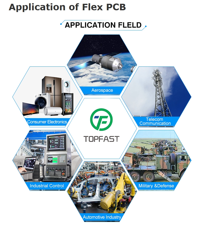
Applications
-
Consumer Electronics
-
Foldable smartphones (hinge-area circuits)
-
TWS earbuds, smartwatches (high-density interconnects)
-
-
Automotive Electronics
-
Vehicle camera modules
-
Battery management systems (BMS flexible circuits)
-
-
Medical Devices
-
Endoscopes, wearable monitors
-
Implantable medical sensors
-
-
Industrial & Communications
-
Industrial robot flexible joint wiring
-
5G mmWave antennas (LCP-based high-frequency FPCs)
-
-
Aerospace
-
Satellite deployable structure circuits
-
UAV lightweight wiring harnesses
-
Frequently Asked Questions (FAQ)
Q1: What file formats do you accept for PCB manufacturing?
We support all industry-standard formats, including:
– Gerber (RS-274X)
– PROTEL (99SE & DXP)
– CAM350
– ODB++ (.TGZ)
– Eagle
– Altium Designer
– PADS
Q2: How do you protect my design files and intellectual property?
We take data security extremely seriously. Your design files are:
– Stored on encrypted servers
– Only accessible to your dedicated project team
– Never shared with third parties without your explicit written consent
– Automatically purged after project completion (unless otherwise requested)
Q3: What payment methods do you accept?
We offer flexible payment options:
Electronic Payments:
– PayPal
– AliPay
– Credit Cards (Visa/MasterCard/UnionPay)
Bank Transfers:
– T/T (Telegraphic Transfer)
– Western Union
– L/C (Letter of Credit)
Q4: What are your shipping options?
We provide global logistics solutions:
Express Shipping (1-5 days):
– DHL
– FedEx
– UPS
– EMS
Bulk Shipping:
– Air freight (>300kg)
– Sea freight (Full container options)
– Can accommodate your preferred freight forwarder
Q5: What is your minimum order quantity?
We specialize in both:
– Prototype quantities (1 piece available)
– High-volume production
No minimum order value requirements
Q6: Can we visit your manufacturing facilities?
We welcome client visits to our facilities:
Main Facility:
Shenzhen, China (ISO 9001 certified)
Secondary Facility:
Guangdong Province, China
Please contact us to schedule a tour with our engineering team
Q7: How do you guarantee PCB quality?
Our comprehensive quality assurance includes:
Testing:
– 100% Electrical Testing (Flying Probe & E-Test)
– Automated Optical Inspection (AOI)
Certifications:
– IPC Class 2/3 standards
– ISO 9001:2015 certified
– UL certified (upon request)
Additional Services:
– Free DFM analysis
– 3D model verification
– Cross-section analysis available
All PCBs come with our quality guarantee and full traceability documentation.