In high-speed digital PCB design, trace impedance control is a critical factor in ensuring signal integrity. As a professional PCB manufacturer, TOPFAST understands that the precise adjustment of outer copper thickness and trace geometry is vital for achieving GHz-level frequencies and data rates exceeding 10 Gbps. This article will analyse the correlation mechanism between copper thickness and impedance from an engineering perspective and provide actionable design guidelines to help engineers achieve stable and reliable performance in high-speed transmission systems.
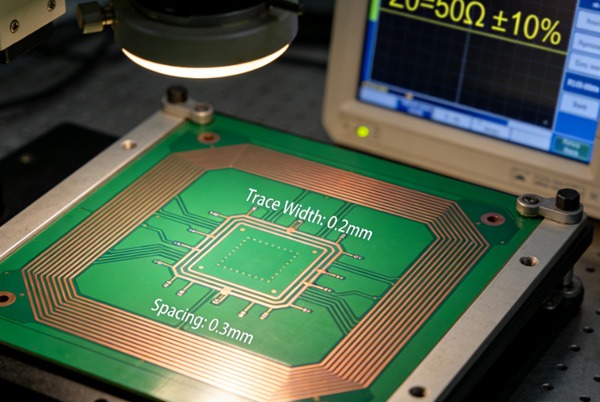
Table of Contents
Why Must We Focus on Trace Impedance?
Trace impedance control is the physical foundation of high-speed digital PCB design. Impedance mismatches can cause signal reflection, ringing, and timing jitter, leading to increased bit error rates. Especially in frequency bands above 5 GHz, even a ±5% impedance deviation can degrade eye diagram closure by more than 40%. Practical cases show that high-speed buses, such as DDR5 memory interfaces and PCIe 5.0, require impedance consistency to be within ±3%.
What Is the Essence of Trace Impedance?
Trace impedance is essentially the wave impedance presented when electromagnetic waves propagate through a transmission line structure, determined by distributed inductance and capacitance. For high-speed digital circuits, the commonly used 50Ω single-ended impedance and 100Ω differential impedance standards are not arbitrary choices but optimal solutions balancing power transmission efficiency, signal attenuation, and noise tolerance.
Industry data indicates that signal integrity issues caused by impedance mismatches account for up to 34% of all problems. For example, a 28 Gbps SerDes interface experienced an 8% impedance fluctuation due to a 2μm deviation in outer copper thickness, ultimately worsening the bit error rate from 10⁻¹² to 10⁻⁸. This fully demonstrates the decisive role of precise impedance control in high-speed systems.
How Does Copper Thickness Affect Impedance?
Quantitative Relationship Between Thickness and Impedance
Copper thickness in PCB manufacturing is typically measured in ounces per square foot (1 oz/ft² ≈ 35μm). The selection of outer copper thickness requires a balance between current-carrying capacity, high-frequency loss, and impedance accuracy. Measured data shows:
- 0.5 oz (17.5μm) Copper Thickness: Suitable for ultra-high-speed signals (>25 Gbps), enabling 3 mil fine trace widths but with higher DC resistance.
- 1 oz (35μm) Copper Thickness: A balanced choice, supporting 5–8 mil trace widths to achieve 50±2Ω impedance control.
- 2 oz (70μm) Copper Thickness: Suitable for power paths, but with a skin depth of only 0.66μm at 10 GHz, resulting in low effective utilisation.
Using impedance calculation models, with a dielectric thickness of 5 mil and Er=4.2:
- 1 oz copper thickness: 8.2 mil trace width yields 50Ω impedance.
- 0.5 oz copper thickness: 6.8 mil trace width achieves the same impedance.
- 2 oz copper thickness: Requires an 11.5 mil trace width to reach 50Ω.
Practical Challenges in the Manufacturing Process
Electroplating, thickening and etching undercut effects during PCB manufacturing can cause the final copper thickness to deviate from the design specifications. Statistics show that a standard 1-oz copper layer may vary between 1.2–1.8 mil (30–45μm) after electroplating, leading to impedance fluctuations of up to ±6%.
Addressing this challenge requires comprehensive measures:
- Implement real-time electroplating monitoring systems to control copper thickness deviations.
- Adjust trace width compensation values based on the etching factor.
- Apply selective electroplating to high-speed signal layers.
Four Key Design Principles: The Foundation of Precise Trace Impedance Control
1. Trace Geometry Optimisation Based on Target Impedance
Recommended design guidelines:
- Single-ended 50Ω traces: When dielectric thickness H ≈ is 5–6 mil, trace width W ≈ is 2.1 × H (for 1 oz copper thickness).
- Differential 100Ω pairs: Optimal coupling coefficient when trace spacing S ≈ 1.5 × trace width.
- Edge-coupled vs. broadside-coupled: Edge coupling is preferred below 10 GHz for easier impedance consistency control.
2. Engineering Considerations for Dielectric Layer Management
Dielectric constant (Dk) and the uniformity of dielectric thickness directly impact impedance stability. Recommended approaches:
- Use low-loss materials (e.g., MEGTRON6, Dk=3.2) instead of FR-4 (Dk=4.2–4.5).
- Adopt symmetrical prepreg structures to avoid lamination warping.
- Reserve ±10% dielectric thickness adjustment margins in stack-up designs.
3. Proactive Strategies for Managing Copper Thickness Variations
A three-phase control method ensures consistency:
- Design phase: Simulate based on the final electroplated thickness rather than the nominal thickness.
- Manufacturing phase: Implement real-time impedance coupon monitoring with ≥3 test points per panel.
- Validation phase: Achieve TDR sampling test coverage of no less than 20%.
4. Systematic Material Selection Methods
Choose material combinations based on frequency requirements:
- <5 GHz: Standard FR-4 materials.
- 5–20 GHz: Medium-loss materials (e.g., TU-768).
- >20 GHz: Ultra-low-loss materials (e.g., RO3003).
Practical Solutions for Addressing Signal Integrity Challenges
Suppressing Impedance Mismatch Reflections
When a signal encounters an impedance discontinuity, the reflection coefficient ρ = (Z₂ – Z₁) / (Z₂ + Z₁). Engineering practices show:
- Tapered trace widths can reduce reflections from 5% impedance transitions to below -35 dB.
- Reference layer voiding in the connector pad areas compensates for capacitive loading effects.
Effective Crosstalk Control Measures
As copper thickness increases, electromagnetic coupling intensifies. Recommended measures:
- 3W rule: Trace spacing ≥ 3 times the trace width reduces far-end crosstalk by 15 dB.
- Ground via arrays: Place shielding vias every 50 mil between differential pairs.
- Non-uniform dielectrics: Use high-Dk materials between adjacent signal layers to increase isolation.
Balancing High-Frequency Losses
Copper thickness selection requires a trade-off between conductor loss and dielectric loss:
- Below 10 GHz: Conductor loss dominates, making increased copper thickness beneficial.
- Above 10 GHz: Skin effect becomes significant, where copper surface roughness is more critical than thickness.
- Actual data: Using very low-profile (VLP) copper can reduce insertion loss at 10 GHz by 20%.
Five Practical Techniques: Complete Control from Design to Manufacturing
- Implement Multi-Physics Co-Simulation
Combine electromagnetic field simulation with process simulation to predict manufacturing deviations’ impact on impedance and optimise designs proactively. - Establish Statistical Process Control Systems
Create Dk/Df databases for each material batch and adjust process parameters in real time to ensure impedance consistency. - Intelligent Application of TDR Testing
Use time-domain reflectometry to create impedance distribution maps, identifying localised anomalies rather than focusing solely on averages. - Digital Design-to-Manufacturing Handover Process
Adopt intelligent data formats to directly transfer impedance requirements and copper thickness tolerances to production equipment. - Early Manufacturing Involvement
Invite manufacturing experts to participate in design reviews during the early stages to avoid costly modifications later.
How TOPFAST Enables Precise Control for High-Speed Transmission
In high-speed digital PCB design, precise control of outer copper thickness and trace impedance has become a core technology determining system performance. By deeply understanding the microscopic impact of copper thickness variations on impedance and implementing full-process control from design to manufacturing, engineers can overcome the challenges of high-speed transmission in the GHz era.
As a professional partner with years of experience in PCB manufacturing, TOPFAST not only provides high-precision impedance control solutions but also creates value for customers through systematic services:
- Professional Design Consultation Support: Impedance design rule libraries based on thousands of successful cases.
- Rapid Prototype Verification Capabilities: 24-hour quick-turn prototyping with comprehensive impedance test reports.
- Batch Production Consistency Assurance: Fully automated optical inspection systems + online impedance monitoring.
- Continuous Technical Training and Exchange: Regular high-speed PCB design seminars sharing the latest practical experiences.
Mastering the art of balancing copper thickness and impedance requires not only theoretical knowledge but also rich practical experience. We recommend that engineers collaborate closely with manufacturing partners from the early design stages, integrating design for manufacturability principles throughout the process. Whether addressing the challenges of 112G PAM4 systems or laying the hardware foundation for next-generation computing platforms, precise impedance control will be the key to success.
PCB Impedance FAQ
A: Impedance mismatch can cause signal reflections, timing disruptions, and increased bit error rates, especially at frequencies above 5 GHz, where a ±5% deviation may degrade signal quality by over 40%.
A: Increased copper thickness reduces resistance per unit length but alters the electromagnetic field distribution, lowering impedance. For example, an 8.2 mil trace width at 1 oz copper achieves 50Ω, while 2 oz copper requires widening to 11.5 mil to maintain the same impedance.
A: For a single-ended 50Ω trace with a 5 mil dielectric thickness and 1 oz copper, the trace width is approximately 8.2 mil. Precise calculations should be performed using simulation tools based on specific dielectric materials (e.g., FR-4 with Dk ≈ 4.3).
A: Copper thickness variation after plating (commonly ±15%)
Etch undercut leading to trace width changes
Inconsistent dielectric layer thickness
Batch variations in material dielectric constant (Dk)
A: Measure trace impedance using TDR (Time Domain Reflectometry)
Recommended sampling test coverage ≥20%
Monitor the process with impedance test coupons
Compare data by sharing simulation models with the manufacturer