Successful PCB design is no longer just about connecting dots; it’s about managing physics. Whether you are working on a simple double-sided board or a complex multi-layer stack-up, following industry-standard principles (such as IPC-2221) is vital. Professional design reduces the risk of signal interference and physical failure, ensuring your project moves smoothly from what is a PCB design to a mass-produced reality.
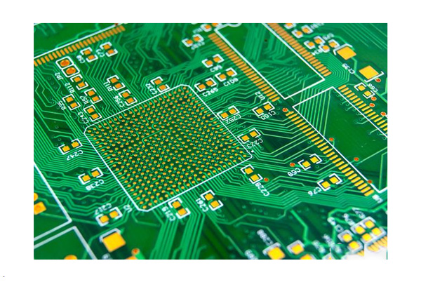
Table of Contents
Core Electrical Integrity Principles
Grounding Strategy: Use a solid ground plane to provide a low-impedance return path for signals, which is a fundamental PCB design optimization strategy.
Signal Integrity (SI): Maintain consistent trace impedance to prevent reflections. Keep high-speed signals away from noisy components.
The 3W Rule: To minimize crosstalk, the distance between traces should be at least three times the width of the trace.
Thermal Management & Component Placement
High-power components generate heat that can degrade performance.
Orientation: Align similar components in the same direction to simplify the soldering process during PCB assembly.
Thermal Vias: Place thermal vias under heat-generating components to conduct heat to internal copper layers.
Component Grouping: Place analog and digital components in separate sections to prevent digital noise from affecting sensitive analog signals.
Design for Manufacturing (DFM)
A “perfect” design is useless if it cannot be manufactured efficiently.
Solder Mask: Ensure proper solder mask expansion to prevent solder bridging during reflow.
Clearance & Spacing: Ensure adequate spacing between traces and board edges to prevent shorts and mechanical damage.
Drill-to-Copper Ratio: Follow manufacturer-specific aspect ratios to ensure via reliability.

How-to: 5 Steps to Implement Professional PCB Design Principles
- Step 1: Plan Your Layer Stack-up
Determine the number of layers based on signal density and power requirements. For complex designs, refer to our Ultimate Guide to PCB Stack-up Design.
- Step 2: Set Design Rules (DRC)
Input your manufacturer’s capabilities (trace width, spacing, hole sizes) into your EDA tool to catch errors early.
- Step 3: Strategic Placement
Place connectors at the edges and sensitive ICs in the center, keeping decoupling capacitors as close to power pins as possible.
- Step 4: Systematic Routing
Route critical high-speed signals first, followed by power traces, and finally general-purpose I/O. Avoid 90-degree corners to reduce EMI.
- Step 5: Final Verification & Export
Perform a final DRC and LVS check before exporting Gerber files. Always include a Readme file with your fabrication requirements.
PCB Design Frequently Asked Questions
A: 90-degree corners can cause signal reflections in high-frequency designs and may act as “acid traps” during the etching process, leading to trace thinning.
A: By following DFM principles, you reduce the need for manual corrections and decrease the scrap rate, which directly lowers the total cost of PCB assembly services.
A: IPC-2221 is the generic standard for printed board design. It provides the industry-recognized criteria for electrical clearances, thermal management, and mechanical properties.
Conclusion
Mastering PCB design principles is an iterative process that balances performance, cost, and manufacturability. By implementing these strategies, you ensure that your electronics are not only functional but also reliable in the long term.
At Topfast, our engineering team reviews every design to ensure it meets the highest industry standards. Ready to start your next project? Explore our PCB Assembly solutions today.