PCB-Montage (PCBA) ist der Schritt, bei dem eine Aus einer nackten Leiterplatte wird eine funktionsfähige ElektronikkarteDie PCB-Fertigung konzentriert sich auf die Phase der Herstellung der nackten Leiterplatte, die die Grundlage des gesamten PCB-Herstellungsprozesses bildet. Sie umfasst Bestückung, Löten und strenge Tests
Die Qualität der Montage wirkt sich direkt aus:
- Elektrische Funktionalität
- Produktzuverlässigkeit
- Produktionsertrag
Unter TOPFASTwird die Baugruppe wie eine ertragsgesteuerter ProzessSie stellen sicher, dass die Tafeln funktional und robust sind.
Hintergrundinformationen über den Zusammenhang zwischen der Leiterplattenbestückung und der Fertigung finden Sie unter: PCB-Fertigung vs. PCB-Montage
Inhaltsübersicht
Oberflächenmontage-Technologie (SMT) Montage
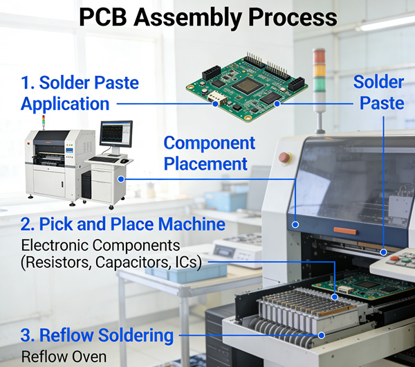
Was ist SMT-Montage?
Die SMT-Bestückung umfasst die Montage oberflächenmontierbare Bauteile direkt auf die Leiterplattenpads aufbringen:
- Lötpaste
- Kommissionier- und Bestückungsautomaten
- Reflow-Löten
SMT ist schnell, präzise und geeignet für Platten mit hoher Dichtedie häufig in Unterhaltungselektronik, Telekommunikation und IoT-Geräten verwendet werden.
SMT-Herausforderungen
- Fine-Pitch-Komponenten erfordern extreme Platzierungsgenauigkeit
- Thermische Spannungen während des Reflow-Prozesses können Leiterplatten beschädigen, wenn die inneren Schichten oder die Kupferbeschichtung nicht einheitlich sind.
- Platten mit hoher Dichte erhöhen die Ertragsempfindlichkeit
Bei TOPFAST wird die SMT-Bestückung sorgfältig mit den Fertigungsdaten koordiniert, um Fehler zu minimieren und den Ertrag zu verbessern.
Montage mit Durchgangsbohrung
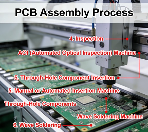
Was ist eine Durchgangslochmontage?
Bei der Durchsteckmontage werden die Bauteile mit den Anschlussdrähten in gebohrte Löcher eingesetzt und verlötet:
- Wellenlöten (Massenlöten)
- Manuelles Löten (für Prototypen oder Kleinserien)
Die Durchgangsbohrung ist nach wie vor weit verbreitet:
- Mechanische Festigkeit
- Hochleistungskomponenten
- Steckverbinder und Großpackungen
Arbeitsablauf bei der Montage durch die Bohrung
- Lochfüllung / Bauteilbestückung - Bauteilanschlüsse in plattierte Löcher einführen
- Löten - Wellen- oder Selektivlöten sichert die Komponenten
- Inspektion - Visuelle oder AOI-Kontrollen für die Lötqualität
Die Qualität von Bohrungen und Beschichtungen wird direkt beeinflusst durch PCB-Bohren vs. Laserbohrenund Verkupferungsprozess erklärt.
Herausforderungen bei Durchgangsbohrungen
- Falsch ausgerichtete oder schlecht plattierte Löcher verringern die Zuverlässigkeit der Lötstellen
- Manuelle Montage erhöht die Arbeitskosten und das Potenzial für menschliche Fehler
- Benötigt mehr Platz auf der Leiterplatte als SMT
TOPFAST kombiniert Präzisionsbohren und Beschichten mit Montageoptimierung um die Ausbeute an Durchgangslöchern zu maximieren.
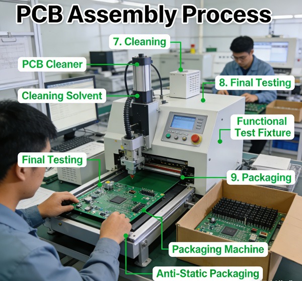
Prüfung und Qualitätskontrolle in der Montage
In-Circuit-Tests (ICT)
ICT-Kontrollen
- Kurze Hosen
- Öffnet
- Korrekte Komponentenwerte
Funktionelle Prüfung
Bei den Funktionstests wird der reale Betrieb simuliert, um zu überprüfen, ob die Karte wie geplant funktioniert.
Die Prüfung ist der letzte Kontrollpunkt, der sicherstellt, dass die Herstellungs- und Montageschritte den Spezifikationen entsprechen. Siehe Ätzprozess und Ertragskontrolle erklärt wie sich die Qualität im Frühstadium auf die Testergebnisse auswirkt.
Überlegungen zur Ausbeute bei der Montage
Ausbeute
- Fertigungsqualität (z. B. innere Schichten, Bohrungen, Beschichtung)
- Genauigkeit der Bauteilplatzierung
- Parameter für das Löten
- Leiterplattendesign (Thermik, Abstände, Pad-Größe)
Ertragreiche Montage reduziert:
- Nacharbeit
- Schrott
- Gesamtproduktionskosten
- Siehe PCB-Fertigung vs. PCB-Montage wie sich Ertragsüberlegungen auf beide Prozesse erstrecken.
Kostenfaktoren bei der Montage
Die wichtigsten Kostentreiber:
- Bauteiltyp und Verpackung
- Plattendichte und Lagenzahl
- Montagevolumen (Prototyp vs. Massenproduktion)
- Prüf- und Inspektionsanforderungen
Die Optimierung der Montage ohne Qualitätseinbußen erfordert enge Abstimmung zwischen Entwurfs-, Herstellungs- und Montageprozessen.
Schlussfolgerung
Bei der Leiterplattenbestückung wird eine nackte Leiterplatte in ein voll funktionsfähiges elektronisches Produkt umgewandelt.
SMT- und Durchgangslochverfahrenin Verbindung mit robusten Tests bestimmen die Zuverlässigkeit des Endprodukts.
Die Integration in die Fertigungsqualität ist von entscheidender Bedeutung:
- Hoher Ertrag
- Kostengünstige Produktion
- Langfristige Zuverlässigkeit
PCB-Bestückungsprozess FAQ
A: Bei der Leiterplattenbestückung werden elektronische Bauteile mit Hilfe von SMT- oder Durchstecktechniken auf einer gefertigten Leiterplatte montiert und anschließend geprüft und getestet.
A: Bei der SMT-Bestückung werden die Bauteile auf der Oberfläche der Leiterplatte montiert, während bei der Durchsteckmontage die Bauteilanschlüsse in gebohrte Löcher eingeführt und verlötet werden.
A: Falsch ausgerichtete Lagen, schlecht gebohrte Löcher oder inkonsistente Beschichtungen können Lötfehler verursachen und die Ausbeute der Baugruppe verringern.
A: Automatisierte optische Inspektion (AOI), Röntgeninspektion, In-Circuit-Testing (ICT) und Funktionstests werden häufig eingesetzt.
A: TOPFAST stimmt Fertigungs- und Montageprozesse aufeinander ab, wendet automatische und manuelle Prüfungen an und nutzt ertragsorientierte Optimierung für eine zuverlässige Produktion.