Finland is much more than the birthplace of global cellular standards; it is a mature industrial powerhouse specializing in Wireless Connectivity (5G/6G), Wearable Health Technology (MedTech), and Industrial IoT. With key tech clusters in Oulu (Radio Valley), Tampere, and Helsinki, Finnish engineering is defined by its demand for extreme reliability and “First-Time-Right” design precision.
For a Finnish Piirilevy (PCB) project to succeed in 2026, it must survive the “Nordic Stress Test”—functioning flawlessly in sub-zero industrial environments while maintaining the micro-miniaturization required for next-gen wearables.
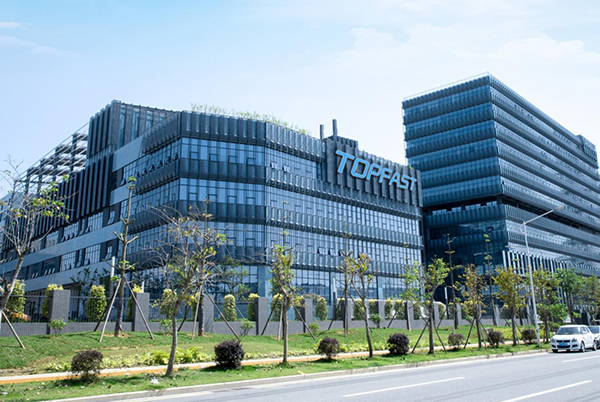
Table of Contents
The Finnish PCB Landscape: Strategic Clusters
The Finnish electronics industry is highly networked, focusing on high-complexity, high-mix production:
Lohja & Salo: Historic manufacturing centers that continue to lead in industrial electronics and automotive sensor assembly.
Oulu (Radio Valley): The epicenter of wireless R&D. Demand here focuses on High-Speed PCBs and RF substrates capable of handling 6G frequency bands.
Helsinki & Espoo: A hub for MedTech (like Oura) and Quantum Computing. This sector requires ultra-fine HDI PCBs and Rigid-Flex PCB solutions for clinical-grade wearables.
Top PCB Partners in Finland
While Finland has a strong domestic base for R&D, the industry relies on a few high-tech pillars:
| Manufacturer | Primary Specialization | Best For… |
| Aspocomp | High-End HDI & QTA | Demanding telecom, defense, and automotive Multilayer PCBs. |
| GPV Electronics (FI) | EMS & Fast Proto | Rapid prototyping and high-mix assembly in the Nordic region. |
| Scanfil | Global EMS | Large-scale industrial and energy sector PCB Assembly. |
Technical Benchmarks for the Finnish Market
To meet the expectations of a Finnish Quality Assurance (QA) manager, your PCBs must address:
- RF Signal Integrity: With Finland’s heritage in cellular tech, precise impedance control and low-loss materials (e.g., Rogers, Panasonic Megtron) are non-negotiable for High-Frequency designs.
- Clinically Validated Reliability: For MedTech, boards must support PCB Surface Finishes like ENEPIG for superior wire bonding and corrosion resistance in wearable applications.
- Sustainability & Traceability: Following the EU’s lead, Finnish firms demand full compliance with REACH, RoHS, and clear conflict-mineral reporting.
Why TopFast is the Preferred Partner for Finnish “Scale-ups”
In Finland, the journey from a “Garage Prototype” to a “Global Product” requires a manufacturing partner that understands the Nordic pace. TopFast serves as a strategic extension for Finnish OEMs:
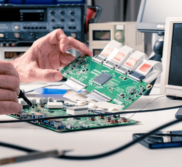
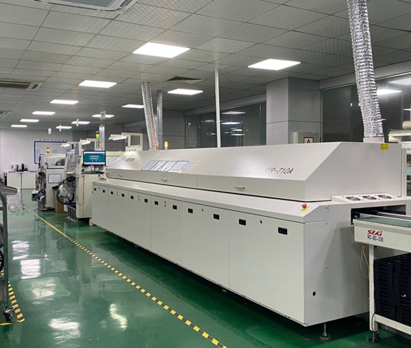
- Bridging Oulu R&D to Volume: We take the complex HDI designs validated in Oulu and scale them into production with a 30-45% cost efficiency compared to local Nordic fabrication.
- Expertise in MedTech Miniaturization: We specialize in the 2-mil trace/space technology required for the latest Finnish health trackers and diagnostic tools.
- Rapid Logistics to HEL/OUL: We provide express shipping to Helsinki-Vantaa and Oulu airports, with door-to-door transit times of 3-5 business days.
PCB Manufacturing by Region
TOPFAST PCB also provides tailored PCB manufacturing services for other regions:
- U.S. PCB Manufacturer
- Canada PCB Manufacturer
- Mexico PCB Manufacturer
- Germany PCB Manufacturer
- France PCB Manufacturer
- UK PCB Manufacturer
- Switzerland PCB Manufacturer
- Netherlands PCB Manufacturer
- Sweden PCB Manufacturer
- Japan PCB Manufacturer
- UAE PCB Manufacturer
This regional network ensures consistent quality, local support, and industry-specific expertise.
Finland Market FAQ
A: Yes. We provide full TDR (Time Domain Reflectometry) and VNA (Vector Network Analyzer) testing for High-Speed PCBs to ensure your RF performance matches your simulations exactly.
A: We provide all necessary EORI-compliant commercial invoices and Certificates of Origin to ensure smooth clearance through Finnish Customs (Tulli).
A: Absolutely. We provide a Free DFM (Design for Manufacturing) Report within 24 hours. Our engineers identify potential yield issues before they become expensive mistakes in the lab.
Next Step for Your Innovation in Finland
In the land of 6G and wearable health, there is no room for “good enough.” You need precision that matches the Finnish spirit of Sisu.
Get an Instant Quote for Delivery to Finland Today — Partner with TopFast to take your Finnish design from a prototype to a global success story.