El cobreado es un paso crítico que convierte los taladros en conexiones eléctricas fiables.
Por muy bien que se diseñe una placa de circuito impreso, un cobreado deficiente puede provocar:
- Conexiones intermitentes
- Vía grietas
- Fallo prematuro del producto
Desde el punto de vista de un fabricante, el cobreado no es sólo un proceso químico, es un proceso de producción. puerta de fiabilidad.
En este artículo se explica cómo funciona el cobreado en la fabricación de placas de circuito impreso, las diferentes etapas del chapado y cómo fabricantes como TOPFAST controlar la calidad del chapado para garantizar un rendimiento a largo plazo.
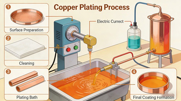
Tabla de contenidos
¿Qué es el cobreado en la fabricación de placas de circuito impreso?
El cobreado es el proceso de depositar cobre en las superficies de las placas de circuito impreso y en el interior de los orificios perforados para crear conexiones eléctricas entre capas.
El chapado tiene dos objetivos principales:
- Permitir la continuidad eléctrica a través de vías
- Conseguir el espesor de cobre necesario para la corriente y la fiabilidad
Tipos de cobreado en la fabricación de PCB
Cobreado químico
El cobreado químico deposita un capa de cobre fina y uniforme sin utilizar corriente eléctrica.
Propósito
- Crear una capa conductora inicial dentro de los orificios perforados
- Preparar la placa de circuito impreso para la galvanoplastia
Espesor típico:
- ~1-3 micras
Este paso es esencial para que las vías sean eléctricamente funcionales.
Cobreado electrolítico
La galvanoplastia utiliza la corriente eléctrica para aumentar el espesor del cobre.
Propósito
- Reforzar mediante muros
- Aumentar el espesor del cobre superficial
- Cumplir las especificaciones de cobre del diseño
La galvanoplastia determina:
- Fiabilidad
- Capacidad de transporte de corriente
- Resistencia mecánica
Proceso de cobreado paso a paso
Paso 1 - Preparación de la pared del orificio
Después de la perforación, las paredes del agujero deben ser:
- Limpio
- Desmeared
- Activado para la deposición de cobre
Una mala preparación provoca una adherencia débil del cobre.
Paso 2 - Deposición de cobre químico
Una fina capa de cobre se deposita químicamente, asegurando:
- Cobertura uniforme
- Continuidad eléctrica
Esta capa es la base de todo el revestimiento posterior.
Paso 3 - Aumento del espesor de la galvanoplastia
El espesor del cobre se aumenta mediante galvanoplastia controlada.
Los parámetros clave son:
- Densidad de corriente
- Química del baño
- Temperatura
- Tiempo de revestimiento
La coherencia es crucial para la fiabilidad.
Espesor del revestimiento y por qué es importante
Vía Espesor de pared
La fiabilidad de la vía depende en gran medida de:
- Espesor mínimo del cobre
- Distribución uniforme
La insuficiencia de cobre puede causar:
- Grietas durante el ciclo térmico
- Circuitos abiertos
Superficie Espesor del cobre
Afecta al cobre superficial:
- Capacidad de corriente de rastreo
- Rendimiento de grabado
- Control de impedancia
En TOPFAST, el espesor del revestimiento se ajusta cuidadosamente a los requisitos de diseño para evitar el exceso o la falta de revestimiento.
Defectos comunes del cobreado
H3: Revestimiento fino
Causado por:
- Tiempo de revestimiento insuficiente
- Mala distribución de la corriente
Reduce la fiabilidad.
Formación del vacío
Pueden producirse huecos en el interior de las vías debido a:
- Limpieza deficiente de los orificios
- Cobertura electrolítica incompleta
Los vacíos son un riesgo importante para la fiabilidad.
Chapado desigual
La distribución desigual del cobre conduce a:
- Debilidad a través de las paredes
- Variación de impedancia
- Pérdida de rendimiento
Cómo afecta el cobreado a la fiabilidad de las placas de circuito impreso
La calidad del cobreado influye directamente:
- Rendimiento en ciclos térmicos
- Resistencia a la tensión mecánica
- Estabilidad eléctrica a largo plazo
En aplicaciones de alta fiabilidad, la calidad del chapado suele ser importante algo más que la apariencia del tablero.
Factores de diseño que influyen en la calidad del metalizado
Desde el punto de vista de la fabricación, el chapado se vuelve más difícil cuando:
- La relación de aspecto es demasiado alta
- El tamaño del orificio es demasiado pequeño
- La distribución del cobre es desigual
- Se utilizan diseños de cobre pesado
La revisión temprana de DFM ayuda a identificar los riesgos del metalizado antes de la producción.
Perspectiva del fabricante: Cómo TOPFAST controla la calidad del metalizado
En TOPFAST, la calidad del cobreado está garantizada:
- Gestión controlada de baños químicos
- Control del espesor en tiempo real
- Análisis transversal regular
- Normas de aceptación alineadas con IPC
- Retroalimentación del diseño basada en DFM
La atención se centra en rendimiento estable y fiabilidad a largo plazono se limita a cumplir unas especificaciones mínimas.
Consideraciones sobre el coste del cobreado
El coste del cobreado aumenta con:
- Grandes necesidades de cobre
- Vías de alta relación de aspecto
- Tolerancias de grosor estrictas
- Especificaciones avanzadas de fiabilidad
La optimización de los requisitos de metalizado puede reducir significativamente el coste de las placas de circuito impreso sin comprometer el rendimiento.
Conclusión
El cobreado es uno de los procesos más críticos en la fabricación de placas de circuito impreso.
Transforma los orificios taladrados en conexiones eléctricas duraderas y define la fiabilidad de las placas de circuito impreso.
Al comprender cómo funciona el cobreado y qué afecta a su calidad, los diseñadores y compradores pueden tomar decisiones más inteligentes que equilibren coste, rendimiento y fiabilidad.
Con procesos controlados y experiencia en fabricación, TOPFAST garantiza una calidad de cobreado que favorece un rendimiento fiable de las placas de circuito impreso durante todo el ciclo de vida del producto..
Lecturas relacionadas
Explicación paso a paso del proceso de fabricación de PCB
Explicación de la fabricación de la capa interior
Taladrado de placas de circuito impreso vs. Taladrado láser
Cobreado FAQ
R: El cobreado crea conexiones eléctricas entre las capas de la placa de circuito impreso y garantiza un espesor de cobre suficiente para la fiabilidad.
R: El metalizado químico crea una capa conductora inicial, mientras que el metalizado electrolítico aumenta el espesor del cobre mediante corriente eléctrica.
R: El grosor del cobre de la vía depende de los requisitos de diseño y fiabilidad, pero debe cumplir las normas IPC para un rendimiento a largo plazo.
R: Las oquedades suelen deberse a una limpieza deficiente de los orificios o a una cobertura incompleta de cobre químico.
R: Un cobreado adecuado mejora la resistencia al estrés térmico, la fatiga mecánica y los fallos eléctricos.