Ensamblaje de PCB (PCBA) es el paso en el que un la placa de circuito impreso desnuda se transforma en una placa electrónica funcional.la fabricación de PCB se centra en la fase de fabricación de placas desnudas, que constituye la base del flujo de trabajo completo de fabricación de PCB. Incluye colocación de componentes, soldadura y pruebas rigurosas
La calidad del montaje afecta directamente:
- Funcionamiento eléctrico
- Fiabilidad del producto
- Rendimiento de fabricación
En TOPFASTEl montaje se trata como un proceso basado en el rendimiento, garantizando que los tableros sean funcionales y robustos.
Para más información sobre la relación entre el montaje de placas de circuito impreso y la fabricación, véase: Fabricación de PCB frente a montaje de PCB
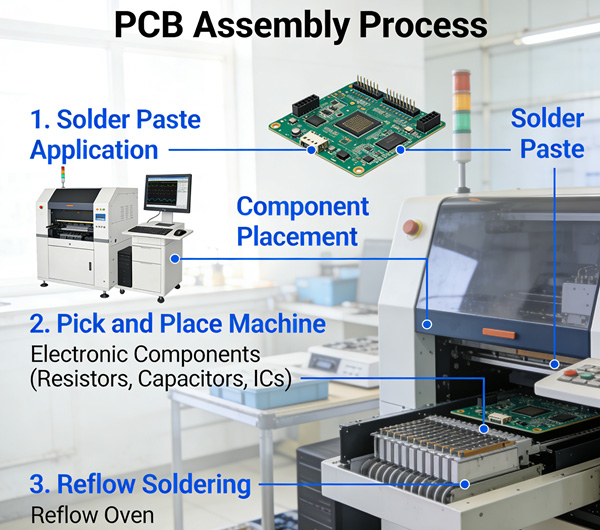
Tabla de contenidos
Tecnología de montaje en superficie (SMT) Montaje
¿Qué es el montaje SMT?
El montaje SMT consiste en montar componentes de montaje superficial directamente sobre las placas de circuito impreso:
- Pasta de soldar
- Máquinas "pick and place
- Soldadura reflow
SMT es rápido, preciso y adecuado para tableros de alta densidadde uso común en electrónica de consumo, telecomunicaciones y dispositivos IoT.
Desafíos SMT
- Los componentes de paso fino requieren una precisión de colocación extrema
- El estrés térmico durante el reflujo puede dañar las placas de circuito impreso si las capas internas o el revestimiento de cobre no son uniformes.
- Las placas de alta densidad aumentan la sensibilidad al rendimiento
En TOPFAST, el montaje SMT se coordina cuidadosamente con los datos de fabricación para minimizar los defectos y mejorar el rendimiento.
Montaje pasante
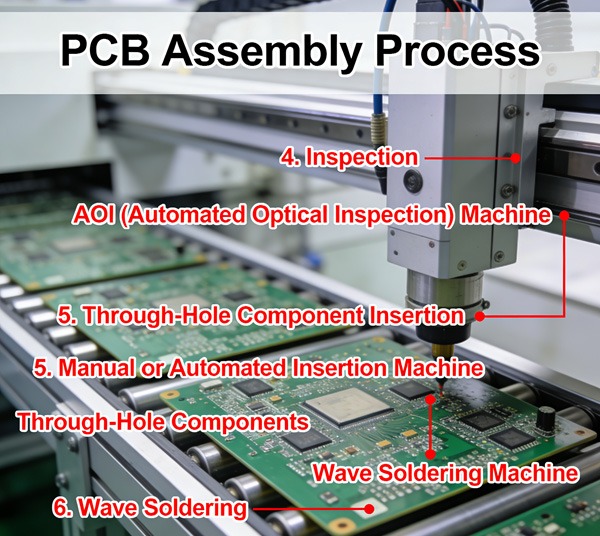
¿Qué es el ensamblaje pasante?
El montaje pasante inserta componentes con cables en orificios taladrados y soldados mediante:
- Soldadura por ola (soldadura en masa)
- Soldadura manual (para prototipos o placas de bajo volumen)
El taladro pasante se sigue utilizando ampliamente para:
- Resistencia mecánica
- Componentes de alta potencia
- Conectores y paquetes grandes
Flujo de trabajo de montaje de orificios pasantes
- Relleno de agujeros / Inserción de componentes - Insertar los cables de los componentes en los orificios chapados
- Soldadura - La soldadura por ola o selectiva fija los componentes
- Inspección - Comprobaciones visuales o AOI de la calidad de la soldadura
La calidad de la perforación y el chapado se ve directamente afectada por Taladrado de placas de circuito impreso vs. Taladrado láserY, Explicación del proceso de cobreado.
Desafíos del agujero pasante
- Los orificios desalineados o mal chapados reducen la fiabilidad de la unión soldada
- El montaje manual aumenta el coste de la mano de obra y la posibilidad de errores humanos
- Requiere más espacio en la placa que SMT
TOPFAST combina taladrado y chapado de precisión con optimización del montaje para maximizar el rendimiento del agujero pasante.
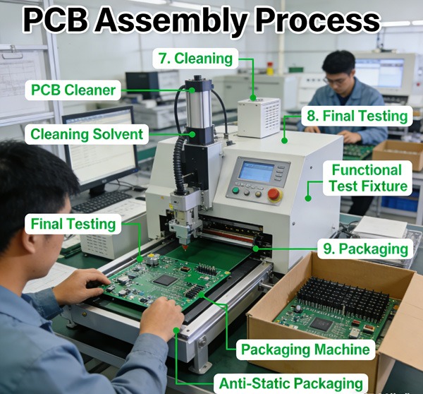
Pruebas y control de calidad en el montaje
Pruebas en circuito (ICT)
Controles de las TIC
- Pantalones cortos
- Abre
- Valores correctos de los componentes
Pruebas funcionales
Las pruebas funcionales simulan el funcionamiento en el mundo real para verificar que la placa funciona según lo diseñado.
Las pruebas son el punto de control final que garantiza que los pasos de fabricación y montaje cumplen las especificaciones. Véase Explicación del proceso de grabado y control del rendimiento de cómo afecta la calidad en las primeras fases a los resultados de las pruebas.
Consideraciones sobre el rendimiento del montaje
Rendimiento
- Calidad de fabricación (por ejemplo, capas internas, perforación, chapado)
- Precisión en la colocación de componentes
- Parámetros de soldadura
- Diseño de la placa (térmico, espaciado, tamaño de las almohadillas)
El montaje de alto rendimiento reduce:
- Vuelva a trabajar
- Chatarra
- Coste global de producción
- Consulte Fabricación de PCB frente a montaje de PCB para ver cómo las consideraciones de rendimiento abarcan ambos procesos.
Factores de coste en el montaje
Principales factores de coste:
- Tipo de componente y embalaje
- Densidad de la placa y número de capas
- Volumen de montaje (prototipo frente a producción en serie)
- Requisitos de ensayo e inspección
Optimizar el montaje sin sacrificar la calidad requiere estrecha coordinación entre los procesos de diseño, fabricación y montaje.
Conclusión
El montaje de placas de circuito impreso convierte una placa desnuda en un producto electrónico totalmente funcional.
Procesos SMT y pasantescombinadas con pruebas rigurosas, definen la fiabilidad del producto final.
La integración con la calidad de fabricación es esencial para lograrlo:
- Alto rendimiento
- Producción rentable
- Fiabilidad a largo plazo
Preguntas frecuentes sobre el proceso de montaje de PCB
R: El ensamblaje de placas de circuito impreso consiste en montar componentes electrónicos en una placa de circuito impreso fabricada mediante técnicas SMT o de taladro pasante, seguidas de inspección y pruebas.
R: Los componentes SMT se montan en la superficie de la placa de circuito impreso, mientras que los pasantes se insertan en orificios taladrados y se sueldan.
R: Las capas desalineadas, los orificios mal perforados o el metalizado irregular pueden provocar defectos de soldadura y reducir el rendimiento del montaje.
R: Se suelen utilizar la inspección óptica automatizada (AOI), la inspección por rayos X, las pruebas en circuito (ICT) y las pruebas funcionales.
R: TOPFAST alinea los procesos de fabricación y montaje, aplica inspecciones automatizadas y manuales, y utiliza la optimización basada en el rendimiento para una producción fiable.