Table of Contents
What Is a Heavy Copper PCB?
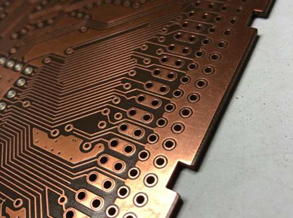
A heavy copper PCB refers to a printed circuit board that uses copper thickness of 3 oz/ft² (105µm) or more, compared to standard PCBs that typically use 1 oz or less.
These boards are specifically designed for applications that require:
- High current-carrying capacity
- Thermal management
- Mechanical durability
If you’re new to PCB fundamentals, you may want to review our PCB Design Guidelines to better understand how copper thickness impacts electrical performance.
Why Use Heavy Copper Instead of Standard PCB?
In many real-world applications, standard copper simply isn’t enough. When current increases, so does heat—and that’s where heavy copper shines.
For a broader overview of manufacturing capabilities, see PCB Manufacturing Capabilities
Key Advantages
1. Higher Current Capacity
Thicker copper allows traces to carry significantly more current without overheating.
2. Better Heat Dissipation
Heavy copper spreads heat more efficiently across the board. For deeper insights, check PCB Thermal Management
3. Improved Mechanical Strength
Thicker copper layers increase resistance to vibration and thermal cycling.
4. Enhanced Reliability
Lower risk of trace burnout or delamination under extreme conditions.
Typical Applications of Heavy Copper PCBs
Heavy copper PCBs are not niche—they’re essential in several industries:
- Power Supplies & Converters
- Electric Vehicles (EV systems)
- Solar Inverters
- Industrial Automation Equipment
- High-Power LED Lighting
- Battery Management Systems (BMS)
If your design involves high current or heat, heavy copper is usually not optional—it’s required.
Copper Thickness Standards
| Copper Weight | Thickness (Approx.) | Classification |
|---|---|---|
| 1 oz | 35 µm | Standard PCB |
| 2 oz | 70 µm | Thick Copper |
| 3 oz | 105 µm | Heavy Copper |
| 4 oz+ | 140 µm+ | Extreme Copper |
When selecting materials, it’s also important to consider thermal stability. Learn more at High TG PCB Materials
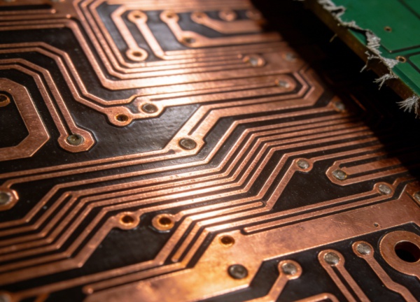
How Heavy Copper PCBs Are Manufactured
Manufacturing heavy copper PCBs is more complex than standard boards. The key difference lies in plating and etching control.
Core Process Differences
1. Special Etching Process
Thick copper is harder to etch cleanly. Manufacturers use step etching or differential etching to maintain trace accuracy.
2. High-Aspect Ratio Plating
Via plating must ensure uniform copper distribution to avoid weak points.
3. Thermal Stress Control
Additional process control is required to prevent warping and delamination.
4. Advanced Lamination
Thicker copper layers require higher pressure and precise lamination cycles.
Design Guidelines for Heavy Copper PCBs
Designing heavy copper boards isn’t just “increase copper weight.” There are trade-offs.
Key Design Considerations
Trace Width vs Current
Even with heavy copper, trace width still matters. Don’t rely only on thickness.
Spacing Rules
Thicker copper requires larger spacing to prevent short circuits during etching.
Thermal Relief Design
Pads connected to heavy copper planes can be difficult to solder—thermal relief patterns are critical.
Via Design
Use larger vias or multiple vias for current distribution.
How to Design a Heavy Copper PCB (Step-by-Step)
- Step 1: Define Current Requirements
Calculate the maximum current for each trace and power path.
- Step 2: Select Copper Thickness
Choose between 3 oz, 4 oz, or higher based on current and thermal needs.
- Step 3: Optimize Trace Geometry
Balance trace width and copper thickness for manufacturability.
- Step 4: Plan Thermal Management
Add copper pours, heat sinks, or thermal vias where needed.
- Step 5: Validate with Manufacturer
Work closely with your PCB supplier to confirm design rules and tolerances.
Common Challenges (and How to Solve Them)
Problem: Difficult Etching Precision
Solution: Increase minimum trace width and spacing.
Problem: Soldering Issues
Solution: Use thermal relief pads.
Problem: Board Warpage
Solution: Ensure balanced copper distribution.
Problem: Higher Cost
Solution: Use heavy copper only where necessary (selective copper design).
FAQ (Frequently Asked Questions)
Typically, any copper thickness above 3 oz (105µm) is classified as heavy copper.
It depends on trace width and temperature rise, but heavy copper can handle significantly higher current than standard PCBs.
Yes, mainly due to:
More complex manufacturing
Lower yield rates
Additional materials
However, they improve long-term reliability and reduce failure risk.
Yes. They can be used in:
Outer layers
Inner layers
Hybrid stack-ups
But it requires advanced manufacturing control.
Heavy copper PCBs are widely used in:
Automotive (especially EV systems)
Renewable energy
Industrial control
Power electronics
Conclusion
If your project involves high current, thermal stress, or harsh environments, heavy copper PCB is not just an upgrade—it’s a necessity.
Need DFM review or quotation?
Our engineering team can help you optimize cost, structure, and reliability before production.