Table of Contents
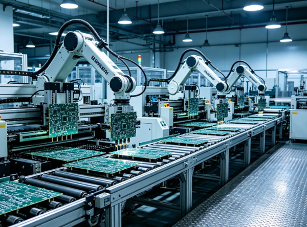
What actually happens inside a PCB factory?
For many engineers and sourcing professionals, PCB manufacturing can feel like a “black box.” Designs are submitted, and finished boards are delivered—but the processes in between are often not fully understood.
In reality, PCB fabrication is a highly controlled, multi-step process that requires precision, consistency, and engineering expertise.
Understanding this process helps you:
- design more manufacturable PCBs
- reduce production risks
- improve communication with suppliers
If you’re new to PCB factories, start here: What Does a PCB Factory Do?
Step 1 — Material Preparation
PCB manufacturing begins with raw materials.
Common materials
- copper-clad laminates (FR4)
- prepreg (insulating bonding layers)
- copper foil
Material quality directly impacts PCB reliability and performance.
Step 2 — Inner Layer Imaging
The circuit pattern is transferred onto the inner copper layers.
Process overview
- apply photoresist
- exposed to UV light
- develop and reveal a pattern
This step defines the internal circuitry of multilayer boards.
More details: Inner Layer Fabrication Explained
Step 3 — Etching
Unwanted copper is removed using chemical etching.
Result
- Only designed copper traces remain
- circuit paths are formed
Process control here is critical to avoid:
- over-etching
- under-etching
Step 4 — Layer Alignment and Lamination
Multiple PCB layers are stacked and bonded.
Key elements
- layer alignment accuracy
- temperature and pressure control
This creates the final multilayer structure.
Step 5 — Drilling
Holes are drilled for vias and components.
Methods
- mechanical drilling (standard PCBs)
- laser drilling (HDI PCBs)
Drilling accuracy affects electrical connectivity and reliability.
Learn more: PCB Drilling vs Laser Drilling
Step 6 — Copper Plating
Copper is deposited inside drilled holes.
Purpose
- create electrical connections between layers
- ensure reliable signal transmission
Poor plating can cause:
- open circuits
- reliability failures
More details: Copper Plating Process in PCB Manufacturing
Step 7 — Outer Layer Imaging and Etching
The outer layers are patterned to complete the circuit.
This step defines:
- component pads
- routing traces
- final circuit structure
Step 8 — Solder Mask Application
A protective layer is applied over the PCB.
Functions
- prevent solder bridging
- protect copper traces
- improve insulation
Design Considerations: PCB Solder Mask Design Guidelines
Step 9 — Surface Finish
Surface finishes are applied to exposed pads.
Common types
- ENIG
- HASL
- OSP
These finishes improve solderability and protect copper.
Step 10 — Testing and Inspection
Final boards undergo quality checks.
Inspection methods
- AOI (Automated Optical Inspection)
- electrical testing (E-test)
- X-ray inspection (if required)
Quality control ensures that boards meet design specifications.
More details: PCB Quality and Reliability Guide
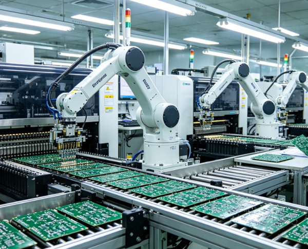
How PCB Factories Ensure Process Stability
A reliable PCB factory maintains strict process control.
Key factors
- standardized workflows
- controlled environment (temperature, humidity)
- equipment calibration
- trained engineering teams
At PCB manufacturers such as TOPFAST, process control and engineering review are essential parts of ensuring consistent manufacturing quality.
How This Process Impacts Your PCB Design
Understanding manufacturing steps helps you design better PCBs.
Design improvements include
- proper trace width and spacing
- manufacturable via structures
- optimized layer stackup
DFM principles are explained in: PCB Design for Manufacturing Guidelines
Conclusion
PCB manufacturing is a complex and highly controlled process involving multiple stages, each of which impacts the final product quality.
By understanding what happens inside a PCB factory, engineers and buyers can make more informed decisions, improve design compatibility, and achieve more reliable production outcomes.
FAQ
A: The PCB manufacturing process includes imaging, etching, lamination, drilling, plating, and finishing.
A: It depends on complexity, but typically ranges from a few days for prototypes to several weeks for mass production.
A: Each step is important, but drilling and plating are especially critical for electrical reliability.
A: Yes, advanced PCB factories support multilayer, HDI, and high-frequency PCB manufacturing.