PCB Design for Manufacturing (DFM) ensures that a circuit board design can be reliably produced using standard fabrication processes.
However, many PCB designs contain DFM violations that may not be detected until manufacturing begins. These issues can result in:
- low production yield
- increased cost
- delays in delivery
- long-term reliability failures
Understanding common PCB DFM violations and how to fix them helps engineers create designs that are both functional and manufacturable.
A full introduction to DFM principles is explained in: PCB Design for Manufacturing (DFM) Guidelines
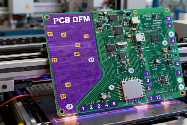
Table of Contents
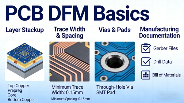
1. Trace Width and Spacing Violations
Problem
Designs often include traces or spacing below manufacturing limits.
Typical issues:
- traces too narrow
- spacing too tight
- inconsistent routing density
Impact
- short circuits
- signal integrity issues
- etching defects
Solution
- follow manufacturer design rules (e.g., ≥ 4 mil trace/spacing)
- maintain consistent routing widths
- Apply DRC rules early in layout
Trace design fundamentals are discussed in: PCB Trace Width and Spacing Design Rules
2. Via Design Errors
Problem
Improper via design is one of the most common DFM violations.
Examples:
- high aspect ratio vias
- small drill sizes beyond capability
- insufficient annular ring
Impact
- poor plating quality
- open circuits
- reduced reliability
Solution
- maintain aspect ratio ≤ 10:1
- ensure sufficient annular ring
- Use standard drill sizes
Detailed via design rules are explained in: PCB Via Design Rules for Reliable Manufacturing
3. Solder Mask Design Issues
Problem
Incorrect solder mask definitions can affect assembly quality.
Common issues:
- mask openings too small
- insufficient solder mask dam
- misalignment between the mask and the pads
Impact
- solder bridging
- poor solder joints
- exposed copper
Solution
- Use proper mask expansion (2–4 mil)
- maintain dam width ≥ 4 mil
- validate mask alignment tolerance
More details are available in: PCB Solder Mask Design Guidelines
4. Component Placement Problems
Problem
Poor component placement can reduce assembly efficiency.
Examples:
- components too close together
- inconsistent orientation
- insufficient spacing for rework
Impact
- placement errors
- reflow defects
- difficult inspection
Solution
- Follow placement spacing guidelines
- align component orientation
- consider assembly process constraints
5. Panelization Design Mistakes
Problem
Improper panel design can cause handling and separation issues.
Examples:
- missing rails
- weak breakaway tabs
- Incorrect spacing between boards
Impact
- board damage during depanelization
- assembly misalignment
- reduced yield
Solution
- Add proper panel rails
- maintain spacing (2–3 mm for routing)
- Choose the correct depanelization method
Panel design details are explained in: PCB Panelization Design Guidelines
6. Drill and Hole Tolerance Issues
Problem
Incorrect hole sizes or tolerances can affect assembly.
Examples:
- hole size is too small
- Incorrect plating requirements
- mismatch with component leads
Impact
- poor component fit
- mechanical stress
- assembly defects
Solution
- define proper finished hole size
- account for plating thickness
- align with component specifications
7. Copper Imbalance and Warpage
Problem
Uneven copper distribution across layers.
Impact
- PCB warpage
- assembly issues
- reliability risks
Solution
- balance copper across layers
- use copper thieving if needed
- maintain symmetric stackup
How to Prevent PCB DFM Violations
Engineers can reduce DFM issues by following a structured workflow.
- Step 1 — Apply design rules early
Set trace, via, and spacing rules at the beginning of layout.
- Step 2 — Perform DRC checks
Ensure compliance with design constraints inside CAD tools.
- Step 3 — Run DFM analysis
DFM checks verify manufacturability beyond basic design rules.
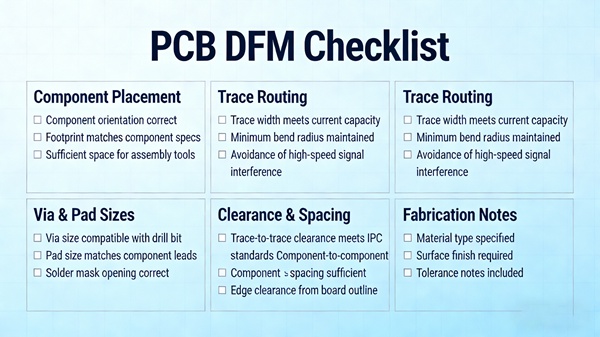
Checklist reference: PCB DFM Checklist Before Sending Gerber Files - Step 4 — Collaborate with manufacturers
Manufacturers review designs and suggest optimizations.
At PCB manufacturers such as TOPFAST, engineering teams typically perform CAM-based DFM analysis before production to identify potential issues early.
Conclusion
PCB DFM violations are a major source of manufacturing problems, but most can be avoided with proper design practices.
By understanding common issues—such as trace spacing, via design, solder mask, and panelization—engineers can significantly improve manufacturability and production efficiency.
Early DFM validation and collaboration with PCB manufacturers are key to achieving reliable and cost-effective PCB production.
FAQ
A PCB DFM violation occurs when a design does not meet manufacturing capabilities, potentially causing production defects or failures.
Trace width/spacing violations and via design errors are among the most common issues.
Yes. DFM issues often reduce yield, require redesign, and increase manufacturing complexity.
DFM checks should be performed during layout and before releasing Gerber files.