Singapore PCB Manufacturer | Reliable PCB Manufacturing Partner for Singaporean Companies
PCB Manufacturing
PCB Manufacturer
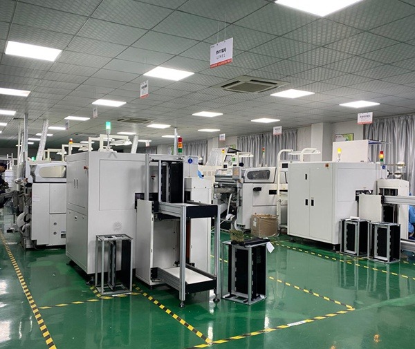
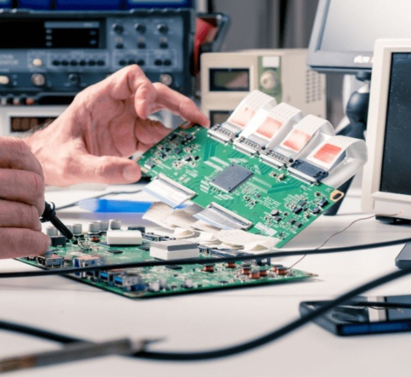
TOPFAST PCB is a trusted Singapore PCB manufacturer with over 17 years of experience. They deliver high-quality, IPC-compliant PCBs for semiconductor, industrial, medical, and telecommunications applications, ensuring reliability across all projects.