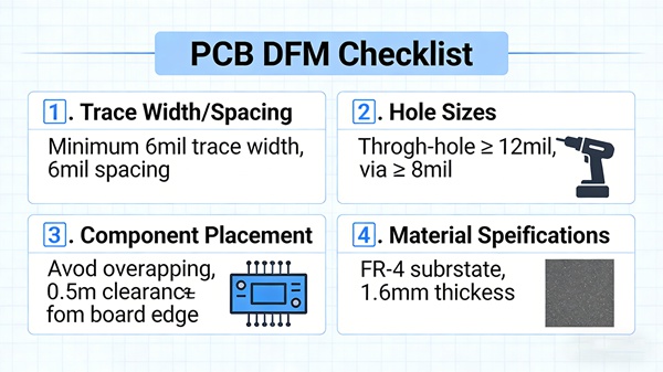
TOPFAST PCB One-Stop Solutions

Blog

PCB Impedance

Outer Copper Layer Thickness and Trace Impedance Control

This article explains how outer copper thickness impacts trace impedance in high-speed PCB design. It covers impedance principles, copper thickness effects (0.5-2oz), key design rules, and manufacturing factors. Discover TOPFAST’s solutions for signal integrity in 5G/AI applications.

PCB Solder Mask Design

Six Common Solder Mask Mistakes Every PCB Designer Should Know

Solder mask design is crucial for PCB reliability. This article covers 6 common errors: insufficient clearance, opening inaccuracies, misalignment, weak solder dams, silkscreen conflicts, and poor testability design. It explains root causes and provides solutions for both standard and high-frequency/high-voltage designs. Includes actionable checklist for better manufacturability.

DFM

PCB Design Must-Check: 5 Critical DFM Issues and How to Avoid Them

This article details the five core DFM issues in PCB design: thermal management, annular rings, board edge clearance, solder mask application, and copper handling. It clarifies the fundamental distinctions between DFM and DRC, providing a full-process checklist and practical parameters. The article emphasizes that early collaboration with manufacturers like TOPFAST can significantly improve yield, reduce costs, and achieve seamless integration from design to manufacturing.

1 14 15 16 44