PCB-Lötmasken-Designrichtlinien für eine zuverlässige Fertigung
Nachrichten
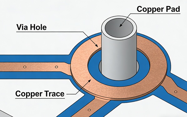
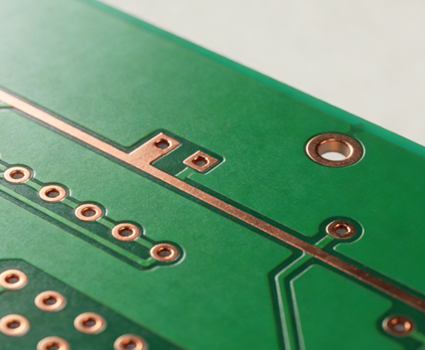
PCB Lötmaske
Die Lötstoppmaske ist eine Schutzschicht, die auf die Oberfläche von Leiterplatten aufgebracht wird, um Lötbrücken zu verhindern und Kupferbahnen zu schützen. Ein korrektes Design der Lötstoppmaske ist für eine zuverlässige Leiterplattenbestückung und einen hohen Fertigungsertrag unerlässlich. In diesem Artikel werden die wichtigsten Richtlinien für das Design von Lötstoppmasken erläutert, darunter Maskenabstand, Maskenausdehnung, Pad-Öffnungen und häufige Layoutfehler. Durch die Einhaltung praktischer DFM-Regeln (Design for Manufacturing) können Ingenieure die Zuverlässigkeit der Bestückung verbessern, Lötfehler reduzieren und die Kompatibilität mit Standard-Leiterplattenherstellungsprozessen sicherstellen.