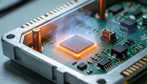
In the rapidly evolving landscape of radio frequency (RF) engineering, microwave technologies, and high-speed telecommunications, the demand for high-performance, compact, and thermally efficient electronic components has never been more critical. At the very heart of these complex high-frequency transmission systems lies the RF power amplifier. This critical component is tasked with amplifying low-power radio frequency signals to the much higher power levels absolutely necessary for effective signal transmission over long distances. As these RF amplifiers become increasingly powerful, handling higher frequencies and operating in smaller form factors, managing extreme heat dissipation and maintaining pristine signal integrity have become the paramount challenges for design engineers. Enter Cavity Printed Circuit Boards (PCBs)—a specialized and highly advanced printed circuit board fabrication technology that strategically incorporates recessed cavities into the board structure to address these exact engineering bottlenecks. This comprehensive article delves deep into the engineering principles behind Cavity PCBs, exploring their benefits, material considerations, and providing actionable insights into designing recessed cavities specifically optimized for RF power amplifiers. Erfahren Sie mehr über Burn-In Boards: High-Density Blind/Buried Vias for High-Pin Count Devices.
The Crucial Role of Recessed Cavities in High-Frequency Design Erfahren Sie mehr über Extreme Miniaturization: 0201m (008004) Component Placement in SMT Assembly.
To understand the value of Cavity PCBs, one must first grasp the physical construction of these specialized boards. A cavity PCB is characterized by deliberate, precisely routed depressions, cutouts, or “pockets” within the board’s multi-layer substrate stackup. Unlike standard through-holes or conventional vias that traverse the entire board, these cavities are carefully depth-controlled. They do not penetrate the entire thickness of the board. Instead, they create a stepped or recessed area within the PCB geometry where active components, such as naked die RF power amplifiers or specialized passive components, can be physically embedded or mounted flush with a specific internal routing layer or the surrounding top surface.
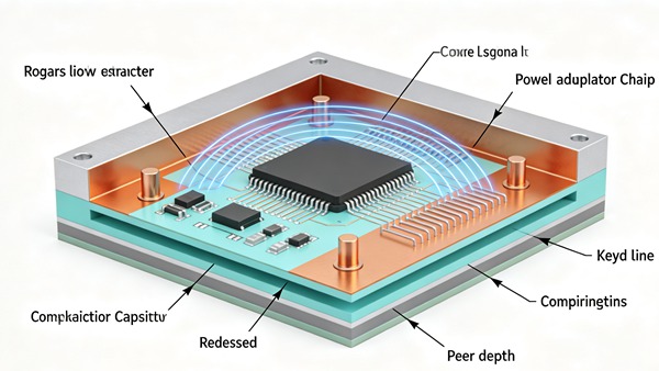
In high-frequency RF engineering, physical dimensions and the physical distance between components dictate electrical performance. The length of interconnection traces, wire bonds, and transition points directly dictate the level of parasitic inductance and capacitance introduced into the circuit. At microwave and millimeter-wave frequencies, even a fraction of a millimeter of excess wire bond can act as an antenna, radiating energy, or act as an inductor, drastically degrading signal integrity, reducing bandwidth, and causing impedance mismatches. By placing the bare die RF power amplifier inside a precisely machined recessed cavity, engineers can align the die’s bonding pads horizontally with the PCB’s signal routing traces. This allows for significantly shortened wire bond lengths between the die and the PCB. This critical reduction in interconnection length minimizes parasitic effects, thereby extending the operational frequency range, reducing return loss, and substantially improving the overall efficiency and linearity of the RF amplifier.
Key Advantages of Cavity PCBs for RF Power Amplifiers Erfahren Sie mehr über Dynamic Flex PCBs: Enhancing Bending Cycles in Wearable Devices.
-
Superior Thermal Management and Dissipation
RF power amplifiers, particularly those built on advanced semiconductor technologies like Gallium Nitride (GaN) or Laterally Diffused Metal Oxide Semiconductor (LDMOS), are notorious for generating substantial, localized heat during operation. In traditional surface-mount designs, this immense thermal load must travel through multiple layers of the PCB substrate (usually FR-4 or high-frequency laminates), which are inherently poor thermal conductors. This thermal bottleneck can lead to component degradation and catastrophic failure. A recessed cavity allows the RF amplifier die to be mounted directly onto a highly conductive copper coin or a solid metal backing plate that forms the bottom floor of the cavity. This architecture provides an ultra-low thermal resistance path, allowing heat to be efficiently and rapidly drawn away from the active junction of the component and dissipated directly into a massive external heat sink or chassis. This direct, unimpeded thermal contact is often the only viable thermal management solution for high-power modern amplifiers. -
Unprecedented Miniaturization and Z-Axis Profile Reduction
In aerospace, defense, satellite communications, and mobile device applications, physical space is at an absolute premium, and weight budgets are strictly enforced. Cavity PCBs enable significant, measurable reductions in the overall Z-axis height of the assembled electronic module. By physically embedding bulky components, such as power amplifiers, circulators, or large capacitors, within the physical thickness of the board itself, engineers can achieve a much flatter, streamlined, and aerodynamic profile. This Z-axis optimization facilitates the design of ultra-thin device enclosures, maximizes volumetric efficiency within complex systems, and allows for tighter stacking of multiple PCB assemblies in confined mechanical housings.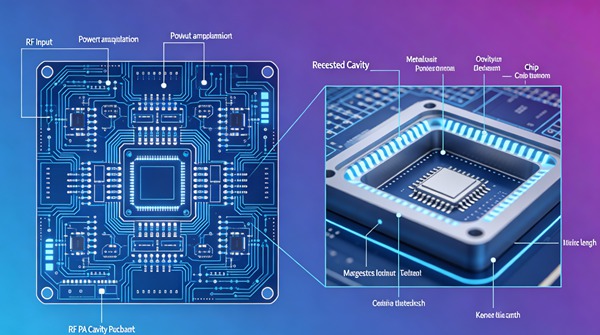
-
Enhanced Signal Integrity and Electromagnetic Shielding (EMI)
Embedding the highly sensitive or noisy RF amplifier within a recessed cavity can also serve to electrically isolate it from external electromagnetic interference (EMI) and prevent it from radiating disruptive noise to adjacent sensitive digital or analog circuits. When the vertical walls and the floor of the cavity are plated with conductive material (typically copper followed by a surface finish like ENIG), they effectively form a localized, partial Faraday cage encompassing the component. Furthermore, as previously mentioned, the dramatically shortened interconnection distances achieved by flush cavity mounting drastically reduce signal degradation, signal reflection, phase noise, and group delay—all of which are critical, tightly controlled parameters in high-frequency RF transmission systems.
Inhaltsübersicht
Material Selection and Design Considerations for Cavity PCBs
Designing a highly reliable cavity PCB is not merely a mechanical exercise; it requires meticulous attention to both electrical and mechanical material parameters, as the fabrication process is significantly more demanding than producing standard multi-layer printed circuit boards.
Advanced Substrate Material Selection: The choice of substrate material is the foundation of high-frequency RF design. Standard FR-4 is rarely sufficient. High-frequency, low-loss laminates such as Rogers RO4000 series, PTFE (Teflon)-based materials, or ceramic-filled hydrocarbon thermoset laminates are typically mandatory. These materials are selected for their tightly controlled, low dielectric constant (Dk) and exceptionally low dissipation factor (Df). When designing a cavity PCB, engineers must also consider the mechanical machinability of these materials. They must understand how these specific laminates behave during the aggressive controlled-depth CNC routing or laser ablation processes used to excavate the cavities, as some materials may fray, delaminate, or leave resin residue.
Precision Depth Control and Manufacturing Tolerances: The Z-axis depth of the recessed cavity must be exceptionally precise to ensure that the embedded die sits at the exact correct elevation relative to the wire bonding pads on the adjacent routing layers. Advanced, highly calibrated CNC routing machines or ultra-precise laser etching techniques are employed by fabricators. However, design engineers must proactively account for inherent manufacturing tolerances (typically ranging from ±1 mil to ±2 mils depending on the process and material) and explicitly specify these critical tolerances in their fabrication data packages.
Metallization and Plating Dynamics: In the majority of high-performance RF applications, the floor and the vertical walls of the recessed cavity must be completely metallized to provide a solid ground reference, robust EMI shielding, or a reliable, solderable surface for die attachment using eutectic bonding or conductive epoxies. The geometric aspect ratio of the cavity (depth versus width) and the complex fluid dynamics of the electroplating chemistry must be carefully considered to ensure uniform, continuous copper deposition within the recessed area, avoiding thin spots or complete voids in the plating.
How to Design Recessed Cavities for RF Power Amplifiers (Step-by-Step Guide)
Beachten Sie diese technischen Vorschriften.
- Determine Component Specifications and Thermal Requirements
Begin the design process by thoroughly and critically analyzing the manufacturer’s datasheet for the specific RF power amplifier bare die. Identify its exact physical dimensions (length, width, and importantly, thickness), the precise pinout and pad locations, expected maximum power dissipation (in Watts), and the absolute maximum operating junction temperature. Calculate the required thermal resistance path from the die junction to the ambient environment to ensure the amplifier operates safely within its thermal limits under maximum load. This critical calculation will explicitly dictate the necessity, thickness, and size of a solid metal coin or an array of thermal vias at the base floor of the proposed cavity.
- Select the Appropriate High-Frequency Substrate Material
Choose a specialized high-frequency PCB laminate that strictly meets the electrical requirements (stable Dk, low Df) of your specific RF operating frequency band. Ensure that the chosen material stackup is highly compatible with complex cavity manufacturing processes, such as mechanical controlled-depth routing, laser ablation, or sequential lamination techniques. It is highly recommended to consult directly with your chosen PCB fabricator’s application engineering team early in this process to verify specific material availability, stackup feasibility, and their in-house process capabilities and tolerance limits.
- Define the Multi-Layer Stackup and Precise Cavity Depth
Design the complete PCB multi-layer stackup to structurally accommodate the required cavity depth. The physical floor of the cavity almost always corresponds directly to a specific internal copper layer that serves as a continuous ground plane, a thermal dissipation pad, or the top surface of an embedded copper coin. Calculate the precise Z-axis depth required so that once the amplifier die is securely mounted, its top-side wire bond pads align perfectly horizontally with the surrounding top-level signal routing traces to minimize the required wire bond loop length.
- Route the RF Signal Traces and Optimize Impedance
Design the critical RF input and output signal traces on the specific PCB layer immediately adjacent to the upper edge of the cavity. Utilize stringent controlled impedance routing techniques (typically targeting 50 ohms for RF systems) and ensure that the physical transition from the PCB trace to the cavity edge is electromagnetically optimized to minimize any impedance discontinuities or reflections. Keep the physical distance between the trace termination edge and the mechanical cavity edge as incredibly short as fabrication tolerances will safely allow.
- Design the Comprehensive Thermal Dissipation Strategy
If your thermal analysis dictates utilizing a solid metal coin for advanced thermal management, design the coin’s dimensions to match or slightly exceed the physical footprint of the amplifier die. Explicitly specify the type of metal (e.g., standard copper or an Invar alloy for critical Coefficient of Thermal Expansion (CTE) matching with the semiconductor die) and define the mechanical method of integration (press-fit insertion, bonded, or fully embedded during lamination). Alternatively, if thermal loads are slightly lower, design a highly dense, mathematically optimized array of plated-through thermal vias in the cavity floor connecting directly to a massive solid ground or thermal plane deeper in the board.
- Specify Strict Tolerances and Generate Fabrication Data
Create highly detailed, unambiguous mechanical drawings and fabrication notes that explicitly define all cavity dimensions, target depths, maximum corner radii (tooling limits), and required minimum/maximum tolerances. Clearly specify whether the vertical cavity walls and the horizontal floor need to be plated and with what specific surface finish (e.g., ENIG, ENEPIG). Generate standard manufacturing files like Gerber RS-274X or ODB++, ensuring that the cavity boundaries, routing paths, and any critical component keep-out zones are clearly and unmistakably marked on a dedicated, clearly labeled mechanical layer. Overcoming Manufacturing Challenges and Ensuring Quality Control The physical production of Cavity PCBs involves highly advanced, specialized fabrication techniques that present unique challenges not found in standard board manufacturing. Mechanical controlled-depth routing requires specialized, frequently replaced router bits and highly calibrated, stable CNC machines to ensure the cavity floor remains perfectly flat and precisely at the target depth. If the dielectric resin in the substrate is not completely and cleanly removed from the internal copper floor, it can severely interfere with the reliability of subsequent die attachment or wire bonding processes. Sequential lamination, a process where sub-assemblies of the board are pressed, drilled, and plated multiple times before the final pressing, is often heavily utilized to create extremely precise, sharp-edged cavities, but this dramatically adds significant time, complexity, and cost to the overall manufacturing cycle. Quality control processes must be equally advanced, including rigorous automated optical inspection (AOI), precise 3D depth measurement utilizing coordinate measuring machines (CMM) or non-destructive laser profilometry, and destructive cross-sectional micro-analysis to definitively verify plating thickness, wall integrity, and overall cavity geometry. Conclusion Cavity PCBs represent a highly sophisticated, absolutely essential engineering solution for overcoming the complex challenges posed by modern, high-power RF power amplifiers. By providing unparalleled superior thermal management capabilities, drastically reducing debilitating parasitic inductance through optimized interconnections, and enabling critical component miniaturization, recessed cavities empower electrical and mechanical engineers to continuously push the recognized boundaries of high-frequency system design. While the specialized design constraints and advanced manufacturing processes are undeniably complex and require close, ongoing collaboration with highly capable PCB fabricators, the dramatic performance benefits in demanding RF applications make Cavity PCBs an indispensable, high-value tool in the critical sectors of global telecommunications, advanced aerospace, and defense technologies.
Designing a cavity for an RF power amplifier requires a systematic approach to ensure both electrical performance and manufacturability. Follow this step-by-step engineering guide. Erfahren Sie mehr über Glass Substrates in PCB: The Future of High-Frequency IC Packaging.
Häufig gestellte Fragen (FAQ)
While both features purposely do not penetrate the entire thickness of the board, a blind via is a small, laser-drilled or mechanically drilled plated hole used exclusively for routing electrical signals between a surface layer and a specific internal layer. In stark contrast, a cavity is a much larger, mechanically routed or laser-ablated depression specifically designed to physically house and embed a discrete component, such as an RF power amplifier bare die, and the cavity walls/floor may or may not be electrically plated depending on the design requirements.
Yes, cavities can certainly be manufactured in standard FR-4 materials, and this practice is somewhat common for low-frequency applications, digital boards, or situations requiring purely mechanical embedding of components for space savings. However, for RF power amplifiers actively operating at high microwave frequencies, advanced low-loss, high-frequency laminates (like Rogers RO4000 or PTFE blends) are virtually always required to maintain strict signal integrity and minimize dielectric losses, despite these specialized materials being generally more challenging to machine and route.
Components, specifically delicate naked dies, are typically attached to the precisely routed floor of the cavity using highly specialized, heat-cured conductive epoxy adhesives, advanced sintered silver pastes, or fluxless eutectic soldering processes. These specific attachment methods are engineered to provide both a remarkably strong mechanical bond to withstand vibration and an exceptionally efficient electrical and thermal interface to the underlying grounded copper plane or the embedded metal thermal coin.
Standard, reliable manufacturing tolerances for mechanical controlled-depth routing are generally specified around ±2 mils (±50 micrometers). However, highly advanced PCB fabricators utilizing state-of-the-art CNC equipment and specialized routing techniques can often achieve tighter, more demanding tolerances of ±1 mil (±25 micrometers). The achievable tolerance heavily depends on the specific substrate material’s physical properties and the overall rigidity of the PCB multi-layer stackup during the machining process.
Recessed cavities significantly improve overall amplifier efficiency primarily by allowing the active die to be mounted perfectly flush with the specific PCB layers dedicated to RF signal routing. This precise physical alignment drastically reduces the required length of the wire bonds connecting the die to the board. Shorter wire bonds directly equate to much lower parasitic inductance. Lower inductance minimizes unwanted signal reflection, dramatically reduces insertion loss, improves impedance matching, and ultimately extends the operational bandwidth and the total power-added efficiency (PAE) of the RF amplifier circuit.