Innehållsförteckning
Introduction to PTFE in High-Frequency PCB Design
Polytetrafluoroethylene (PTFE), widely recognized by the brand name Teflon, has become the substrate of choice for high-frequency, radio frequency (RF), and microwave printed circuit boards (PCBs). In an era where telecommunications, aerospace, and advanced driver-assistance systems (ADAS) demand signal frequencies extending well into the millimeter-wave (mmWave) spectrum, standard FR-4 laminates fall drastically short. PTFE fills this gap, offering an exceptionally low dielectric constant (Dk) and a remarkably low dissipation factor (Df). These electrical properties ensure minimal signal loss, reduced phase distortion, and excellent impedance control at frequencies exceeding 10 GHz. Lär dig mer om Probe Cards: Design and Manufacturing of Multi-Layer Test Interface Boards.
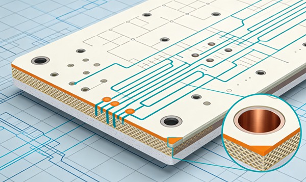
However, the very molecular structure that grants PTFE its unparalleled electrical performance—long chains of carbon atoms completely saturated by fluorine atoms—also renders it one of the most difficult materials to process in a PCB manufacturing environment. The strong carbon-fluorine bonds create a chemically inert surface with extremely low surface energy, meaning nothing naturally adheres to it. Furthermore, pure PTFE is relatively soft and exhibits significant dimensional changes under thermal stress. To combat these physical shortcomings, laminate manufacturers often reinforce PTFE with woven glass fiber or load it with ceramic fillers. While these reinforcements improve mechanical stability, they introduce their own distinct set of challenges during drilling, routing, and plating.
Understanding the intricacies of PTFE PCB manufacturing is critical for design engineers and fabrication facilities alike. A slight deviation in the processing parameters can lead to catastrophic failures, such as delamination, through-hole plating voids, or signal integrity degradation. This article delves deeply into the manufacturing and plating challenges associated with PTFE substrates, providing actionable engineering insights into overcoming the inherent hurdles of this advanced material.
The Physical and Chemical Realities of PTFE Substrates
Before exploring specific manufacturing processes, it is essential to understand the material science dictating PTFE’s behavior on the fabrication floor.
Dimensional Stability and Coefficient of Thermal Expansion (CTE)
Pure PTFE has a high Coefficient of Thermal Expansion (CTE), particularly in the Z-axis, which can lead to excessive stress on plated through-holes (PTH) during thermal cycling or soldering operations. While ceramic fillers and glass weaves mitigate this, the CTE mismatch between the PTFE substrate, the copper cladding, and the glass reinforcement remains a critical engineering consideration. The material is also susceptible to “cold flow” or creep under sustained pressure, which can complicate mechanical fastening and lamination processes. Manufacturers must strictly control temperatures and apply uniform pressure to prevent substrate deformation.
Chemical Inertness and Surface Energy
PTFE’s defining characteristic is its chemical inertness. It resists attacks from strong acids, bases, and organic solvents. While excellent for environmental reliability, this inertness means that standard chemical desmear and surface activation processes used for FR-4 are completely ineffective on PTFE. The material’s low surface tension repels aqueous plating solutions, necessitating aggressive and highly specialized surface treatments to achieve the copper adhesion required for reliable PTH metallization.
Drilling and Hole Preparation Challenges
The mechanical processing of PTFE, particularly drilling via holes, requires a fundamental departure from standard FR-4 parameters.
Drill Smear and Fraying
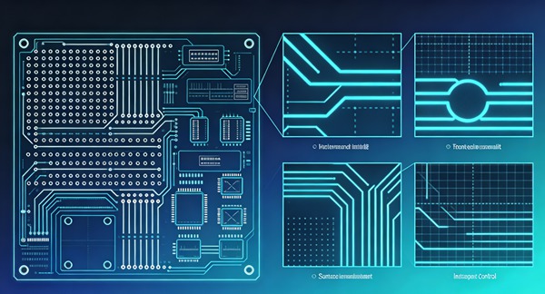
Because pure PTFE is relatively soft and thermoplastic, the heat generated by the friction of a drill bit can easily cause the material to melt and smear across the inner copper layers, creating an insulating barrier that prevents electrical connection. Conversely, if the PTFE is heavily reinforced with glass fiber, the differing hardness between the soft PTFE and the hard glass can cause the glass fibers to fray or tear out, leaving a rough hole wall that is exceptionally difficult to plate uniformly. Lär dig mer om Solder Voiding under QFN: Root Causes and Thermal Profiling Solutions.
To mitigate these issues, engineers must optimize drill bit geometries, utilizing specialized under-cut bits or varying flute angles to facilitate chip evacuation. Feeds and speeds (spindle RPM and chip load) must be strictly controlled to minimize heat generation. Often, the drilling process requires precise peck drilling techniques or the use of specialized backup and entry materials to maintain hole wall integrity.
Dealing with Ceramic Fillers
When drilling ceramic-filled PTFE laminates, drill bit wear accelerates exponentially. The abrasive nature of the ceramic particles dulls standard tungsten carbide bits rapidly, necessitating frequent tool changes to prevent poor hole quality. Monitoring tool life and implementing strict replacement schedules is mandatory to avoid the catastrophic quality issues associated with dull drills, such as excessive smear, nail-heading of inner layers, and wandering via holes. Lär dig mer om Automotive PCB Reliability: Understanding IPC-6012 Class 3 vs Class 3A.
Surface Activation and Plating (Metallization)
Once the holes are drilled, the most critical and challenging phase of PTFE PCB manufacturing begins: preparing the inert hole wall for electroless copper deposition.
The Necessity of Surface Treatment
Because electroless copper will not adhere to untreated PTFE, the surface of the hole wall must be chemically or physically altered to increase its surface energy and create microscopic mechanical anchoring points. Standard alkaline permanganate desmear, which effectively oxidizes and removes epoxy smear in FR-4, does absolutely nothing to PTFE.
Sodium Etchant (Tetra-Etch) Processing
The traditional and highly effective method for activating PTFE is the use of a sodium-napthalene complex or a sodium-ammonia solution (often referred to commercially as Tetra-Etch). This incredibly aggressive chemical treatment strips fluorine atoms from the carbon backbone at the surface of the PTFE, leaving a carbon-rich, unsaturated surface that is highly receptive to subsequent plating chemistries. The process turns the normally white PTFE surface a dark brown or black.
While highly effective, sodium etchants are exceedingly hazardous. They are highly reactive with water, require extreme safety precautions, have a short bath life, and pose significant environmental and disposal challenges. Furthermore, over-etching can degrade the electrical properties of the substrate, while under-etching results in catastrophic plating voids.
Plasma Desmear and Activation
Due to the hazards of wet sodium processing, plasma treatment has become the preferred method for many advanced fabrication facilities. In a vacuum chamber, a mixture of gases (typically containing hydrogen, nitrogen, and sometimes oxygen or CF4) is excited by an RF field to create a highly reactive plasma. The plasma ions bombard the hole wall, simultaneously cleaning away drill smear and modifying the surface chemistry of the PTFE to improve wettability and adhesion.
Plasma treatment provides excellent, repeatable results and eliminates the handling of hazardous sodium complexes. However, plasma equipment requires a massive capital investment, and the process is fundamentally a batch operation, which can create a bottleneck in high-volume production environments. Achieving uniform plasma distribution across densely packed panels with high aspect ratio holes requires meticulous optimization of gas flows, pressure, RF power, and cycle times.
Multilayer Lamination Challenges
Constructing multilayer PCBs using PTFE substrates introduces another layer of complexity. The lamination process requires bonding distinct layers of PTFE together, often utilizing specialized bonding films or prepregs.
High-Temperature Bonding
Unlike standard epoxy prepregs that cure at around 170°C to 190°C, PTFE laminates often require fusion bonding at temperatures exceeding 350°C, approaching the melting point of the PTFE itself. These extreme temperatures demand specialized, high-temperature lamination presses. The thermal expansion during this high-temperature cycle must be carefully managed to prevent misregistration between layers.
Bonding Films (FEP and PFA)
When pure fusion bonding is not feasible, specialized thermoplastic bonding films such as Fluorinated Ethylene Propylene (FEP) or Perfluoroalkoxy (PFA) are used. These materials have slightly lower melting points than PTFE (around 260°C to 290°C) and flow under pressure to encapsulate inner layer copper traces and bond the substrates together. The rheology (flow characteristics) of these films must be precisely understood; excessive flow can cause dielectric thickness variations, thereby altering the designed impedance, while insufficient flow leads to air entrapment and delamination.
How to Manufacture and Plate PTFE PCBs (Step-by-Step Guide)
Följ dessa tekniska riktlinjer.
- Material Preparation and Baking
Before any mechanical processing begins, the PTFE laminates must undergo a rigorous baking cycle. Because PTFE can absorb minute amounts of moisture (especially when combined with glass or ceramic fillers), the boards are baked in specialized ovens. This step relieves internal stresses accumulated during the raw material manufacturing process and drives out any trapped moisture, which could otherwise vaporize during lamination or soldering and cause blistering or delamination.
- Specialized Drilling Operations
The panels are loaded onto CNC drilling machines utilizing optimized parameters. Spindle speeds are generally reduced, and chip loads are carefully calibrated to prevent localized melting of the thermoplastic PTFE. Specialized drill geometries with specific undercut angles are employed, and drill hit counts are strictly limited, especially on ceramic-filled laminates, to prevent dulling and subsequent hole wall tearing.
- Hole Wall Cleaning and Smear Removal
Standard desmear chemistries are bypassed. If the laminate contains a combination of FR-4 and PTFE (a hybrid board), a careful sequential desmear may be required, but for pure PTFE, mechanical or plasma cleaning is paramount. Any loose debris or frayed glass fibers are removed using high-pressure water rinses or ultrasonic cleaning.
- Surface Activation via Plasma Treatment
The drilled panels are placed into a vacuum plasma chamber. A precise mixture of gases (e.g., Nitrogen and Hydrogen) is introduced, and an RF field strikes the plasma. The reactive ions bombard the PTFE hole walls, defluorinating the surface on a microscopic level. This process modifies the inherently hydrophobic surface, rendering it hydrophilic and increasing its surface energy to accept plating chemistries.
- Elektrolös kopparbeläggning
Immediately following plasma activation, the panels enter the electroless copper line. The newly active carbon-rich surface allows the palladium catalyst to adhere. The panels are submerged in the electroless copper bath, where an autocatalytic chemical reaction deposits a thin, uniform layer of pure copper (typically 20 to 50 microinches) onto the entire hole wall, establishing the initial conductive path from the top to the bottom of the via.
- Electrolytic Panel or Pattern Plating
With the electroless copper seed layer established, the boards are processed through standard electrolytic copper plating. Using direct current, copper is electroplated onto the surface and inside the holes to achieve the final required copper thickness (typically 1 mil or 25 microns). The throwing power of the plating bath must be optimized to ensure uniform copper distribution in high aspect ratio via holes without burning the surface copper.
- High-Temperature Multilayer Lamination
If the board is a multilayer design, the etched inner layers are stacked with specialized bonding films (such as FEP or PFA). The book is placed into a high-temperature lamination press. The press cycle involves ramping the temperature up to approximately 290°C (or higher for direct fusion), applying vacuum to evacuate air, and engaging precise hydraulic pressure to flow the bonding film and fuse the layers into a solid, monolithic composite structure.
The following guide outlines the highly specialized engineering process required to successfully fabricate and plate a high-frequency PTFE circuit board.
Summary of Engineering Considerations
Successfully navigating the challenges of PTFE PCB manufacturing requires a holistic approach to process engineering. Every step, from the initial CAD layout considering CTE mismatches, through to the specialized drill feeds, plasma activation cycles, and extreme lamination temperatures, must be meticulously controlled. By understanding the fundamental material science of polytetrafluoroethylene, PCB fabrication engineers can reliably produce the high-performance, low-loss interconnects required by today’s most demanding RF and microwave technologies. Lär dig mer om Dynamic Flex PCBs: Enhancing Bending Cycles in Wearable Devices.
Ofta ställda frågor (FAQ)
Standard FR-4 desmear relies on an alkaline permanganate solution to oxidize and dissolve epoxy resins. PTFE is chemically inert and completely resistant to strong oxidizers and alkaline solutions. Permanganate will not alter the PTFE surface, meaning the subsequent electroless copper will fail to adhere, resulting in voided plated through-holes.
While both methods effectively activate the PTFE surface for plating, plasma treatment is significantly safer and more environmentally friendly. Sodium etchants are extremely hazardous, highly reactive, and require costly disposal procedures. Plasma is a dry, clean process that utilizes easily managed gases and poses drastically lower safety risks to manufacturing personnel.
PTFE has a high Coefficient of Thermal Expansion, particularly in the Z-axis (thickness). During thermal cycling (such as environmental temperature changes or soldering processes), the PTFE expands significantly more than the copper plating inside the via holes. This CTE mismatch places immense stress on the copper barrel, which can lead to fatigue, barrel cracking, and ultimately, open circuits.
Hybrid PCBs are designed to balance cost and performance. PTFE is expensive and difficult to process, so it is often only used for the specific outer or inner layers carrying critical high-frequency RF signals. The remaining layers, which might only carry low-frequency power or digital control signals, are constructed from cheaper, easily processable FR-4. This approach requires complex, sequential manufacturing processes to handle the vastly different material properties within the same board.
FEP (Fluorinated Ethylene Propylene) and PFA (Perfluoroalkoxy) are thermoplastic fluoropolymers closely related to PTFE. They are used as bonding films (adhesives) in multilayer PTFE PCB lamination because they possess slightly lower melting points than pure PTFE while maintaining excellent high-frequency electrical characteristics. Under heat and pressure, they melt and flow to bond the individual PTFE laminate layers together without degrading the board’s RF performance.