What Determines PCB Quality? Manufacturing and Design Factors Explained
News
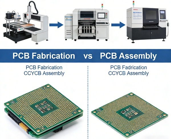
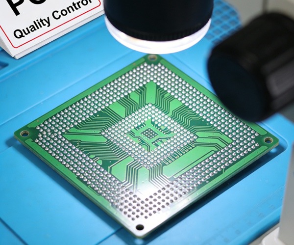
PCB Quality
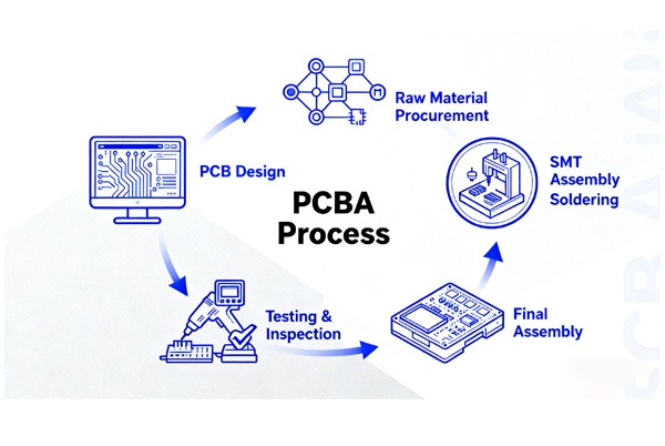
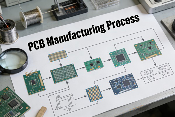
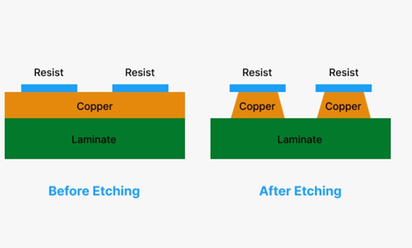
PCB quality hinges on material selection, design choices, manufacturing precision, and rigorous quality control. This guide details these key factors to ensure reliable and high-performance circuit board production.