Multilayer PCB Manufacturing and Quality Control
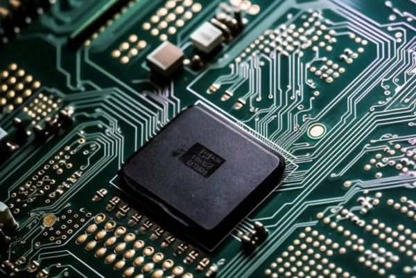
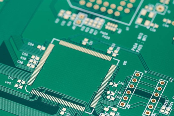
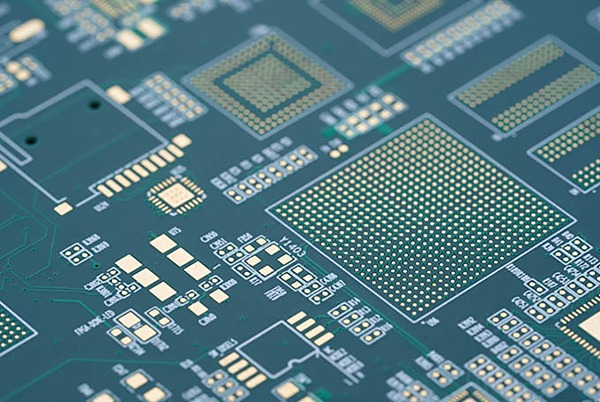
The quality of multilayer PCBs is determined by factors other than the number of layers. The misconception that “more layers mean better quality” should be dispelled. Reliability hinges on stacking design, material selection, and process control.